Image Generated Using DALL-E
Yield And Wafer Excursions:
In the complex world of semiconductor manufacturing, maintaining a high yield – the percentage of functional devices from a batch of wafers – is the ultimate goal. However, various challenges, including wafer excursions, can impede this process.
These wafer-level deviations from the standard processing environment often impact yield by introducing defects that affect the final product’s performance and reliability. Thus, in addition to several yield-related learnings, it is also crucial to understand wafer excursions and how they correlate to introducing new semiconductor products.
Premier On Wafer Excursions:
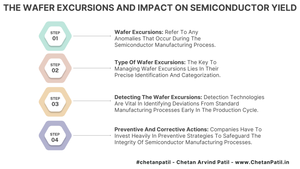
Wafer excursions refer to any anomalies that occur during the semiconductor manufacturing process, deviating from the controlled conditions expected in production.
These can range from several fluctuations in material, mask, fabrication step, equipment, etc. The consequences of these excursions can be severe, creating defective chips that fail to meet the required specifications. Thus, they impact customer satisfaction (from a process point of view) and raise concerns about product quality.
Type Of Wafer Excursions:
The key to managing wafer excursions lies in their precise identification and categorization. Each type, with its distinct causes and effects, requires this level of detail. It is through this process that we can ensure the correct preventive measures and responses are implemented.
There are four main categories of wafer excursions based on their origin and nature.
| Type of Excursion | Description |
|---|---|
| Process Excursions | Deviations in processing parameters such as temperature, pressure, chemical concentration, or deposition rates. For example, over-etching leading to faulty circuits. |
| Equipment-Related Excursions | Faults or malfunctions in manufacturing equipment like lithography tools, etchers, or deposition systems that lead to inconsistent processing across the wafer. |
| Environmental Excursions | Variations in the cleanroom environment, such as changes in temperature, humidity, or particulate contamination, which can adversely affect the processes. |
| Material Excursions | Issues with the materials used in the process, such as contamination, incorrect mixing, or improper handling of dopants, metals, or gases. |
Understanding these excursions is crucial for setting up effective monitoring systems, developing robust manufacturing protocols, and training personnel to handle and respond to potential deviations promptly.
With this knowledge, manufacturers can significantly enhance their ability to maintain high yields and produce reliable, high-quality semiconductor products.
Detecting The Wafer Excursions:
Advanced detection technologies are vital in identifying deviations from standard manufacturing processes early in the production cycle. These technologies enable manufacturers to intervene promptly, correcting issues before they escalate into significant yield losses.
Here is a comprehensive table outlining the various detection techniques used in semiconductor manufacturing to identify and address wafer excursions:
| Detection Method | Technology and Application |
|---|---|
| Inline Data | Tools that measure critical dimensions, film thicknesses, and other physical to die level characteristics of wafers during manufacturing. These real-time measurements help in detecting deviations promptly. |
| Defect Inspection Systems | Utilize various imaging techniques, such as optical or electron microscopy, to identify physical defects on the wafer surface. Capable of detecting particulate contamination, pattern anomalies, and other defect types. |
| Electrical Testing | Conducted at various stages of the manufacturing process to assess the electrical functionality of circuits. This testing helps identify electrical failures that might indicate underlying physical or process defects. |
| Environmental Monitoring | Sensors continuously monitor the cleanroom environment for particulates, chemical vapors, temperature, and humidity, providing alerts to any conditions that could destabilize the process. |
Integrating advanced detection techniques into semiconductor manufacturing processes is crucial for minimizing the impact of wafer excursions. These technologies enhance the ability to detect and correct deviations quickly and contribute to the overall efficiency and cost-effectiveness of semiconductor manufacturing.
These detection methods will evolve as technology advances, offering even greater precision and reliability in monitoring manufacturing processes.
Impact of Wafer Excursions:
The impacts of excursions are far-reaching, affecting yield and the long-term reliability of semiconductor devices. It is imperative that manufacturers understand these impacts and implement effective strategies to mitigate risks and enhance product quality.
The table below captures the primary impacts of wafer excursions on semiconductor manufacturing.
| Impact Category | Description |
|---|---|
| Yield Reduction | Small deviations in the manufacturing process, especially in critical stages like photolithography, can lead to significant yield losses. |
| Reliability Issues | Excursions can introduce latent defects into devices, which may not cause immediate failures but can decrease the devices’ long-term reliability. |
| Scrap and Rework | In severe cases, excursions can necessitate the scrapping of entire batches of wafers or require costly rework to salvage usable components. |
These disruptions can have serious consequences, from reduced yield and reliability to increased costs due to scrap and rework. For semiconductor manufacturers, quickly detecting and effectively responding to wafer excursions is not just a technical necessity.
It is a critical business strategy that directly impacts profitability and market competitiveness.
Preventive, Corrective Actions And Take Aways For Wafer Excursions:
In the field of semiconductor manufacturing, precision and reliability are of utmost importance. To ensure efficient production, it is essential to implement robust preventive strategies.
These strategies are designed to minimize the occurrence of wafer excursions by addressing potential issues before they impact the production process. Below is a table outlining the key preventive measures.
| Strategy | Description |
|---|---|
| Process Control Enhancements | Advanced Process Control (APC) systems utilize real-time data from inline metrology to automatically adjust process parameters, ensuring stable and controlled manufacturing conditions. |
| Predictive Maintenance | This approach uses data analytics to predict potential equipment failures before they occur, thereby reducing the risk of equipment-related excursions. |
| Improved Material Handling Protocols | Strict protocols ensure that all materials are handled, stored, and used under controlled conditions to prevent contamination or degradation, maintaining the integrity of the manufacturing process. |
Companies invest heavily in preventive strategies to safeguard the integrity of semiconductor manufacturing processes. These strategies are designed not only to detect and correct wafer excursions but also to prevent their occurrence. By implementing advanced systems and protocols, manufacturers can maintain a high level of process control and material integrity, which are crucial for minimizing disruptions and ensuring consistent product quality.
To conclude, wafer excursions pose significant challenges in the semiconductor manufacturing, affecting everything from yield to device reliability. Through a comprehensive understanding of the types and impacts of these excursions, coupled with advanced detection techniques and robust preventive strategies, manufacturers can effectively manage and mitigate their effects.
The proactive management of wafer excursions is not just about enhancing yield, but about ensuring the production of high-quality, reliable semiconductor devices. This holistic management, which is the key to maintaining the operational efficiency and economic viability of semiconductor manufacturing in an increasingly demanding and competitive market, puts the control back in the hands of manufacturers.


