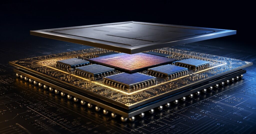
#chetanpatil – Chetan Arvind Patil

Category: MANUFACTURING

Semiconductor Data Is Becoming The Industry’s Most Valuable Asset

Image Generated With GPT Image 2.0 Data Is Becoming A Strategic Investment For decades, semiconductor investments have focused on fabs, process technologies, manufacturing equipment, and packaging innovations. While these remain critical, another area is demanding increasing attention: semiconductor data. Every stage of the semiconductor lifecycle generates valuable information, from design

Read More

The Data Movement Is Becoming The Next Semiconductor Scaling Challenge

Image Generated With GPT Image 2.0 Compute Scaling Alone Is No Longer Enough For decades, semiconductor progress was driven primarily by transistor scaling. Smaller transistors enabled higher compute density, faster performance, and lower power consumption, allowing continuous system level improvements across multiple generations of computing infrastructure. Today, that scaling model

Read More

The State Of Semiconductor Agents

Image Generated With GPT Image 2.0 State Of Silicon Agents Artificial intelligence in semiconductors is rapidly moving beyond copilots and analytics dashboards. The industry is now entering the era of semiconductor agents, where AI systems can autonomously analyze data, optimize workflows, coordinate engineering tasks, and increasingly make operational decisions across

Read More

The Post-Scaling Semiconductor Shift Where Packaging, Data, And Yield Define Competitive Advantage

Image Generated With GPT Image 2.0 System-Level Scaling Beyond Moore’s Law The semiconductor industry is moving beyond traditional transistor scaling. Rising fabrication costs, power density limits, and reticle constraints are making monolithic scaling increasingly difficult. Instead of relying only on smaller transistors, the industry is shifting toward system-level integration through

Read More

The Silicon Photonics And Semiconductor Scaling Trilemma

Image Generated With GPT Image 2.0 Semiconductor Scaling Is Becoming A System Problem The semiconductor industry is entering a phase in which scaling is no longer defined solely by transistor density. For decades, advances in lithography and process scaling have improved performance, power efficiency, and integration density. Smaller transistors enabled

Read More

The Computational Lithography Skills That Bridge Physics, Algorithms, And Semiconductor Manufacturing

Nano Banana From Optical Limits To Computational Correction Computational lithography has become central to advanced semiconductor manufacturing. Traditional optical scaling is reaching its physical limits. At nanometer dimensions, patterns designed on masks cannot be directly transferred onto silicon with sufficient fidelity. This is due to diffraction, interference,

Read More

The Role Of The Semiconductor Industry In Enabling Co-Compute Systems

ChatGPT Images 2.0 Shift From Monolithic Compute To Collaborative Systems For decades, compute scaling followed a predictable path: pack more transistors onto a single die, increase frequency, and extract higher performance from a centralized processor. That model is now structurally breaking down. The limiting factor is no

Read More

The Emergence Of Data Platforms In Semiconductor Manufacturing

Nano Banana Fragmented Data To Integrated Manufacturing Intelligence Semiconductor manufacturing has always been data-intensive, but historically this data has been fragmented across multiple systems, including equipment logs, yield databases, test data, MES, and enterprise systems. These systems evolved independently and were optimized for specific functions rather than

Read More

The Semiconductor Vertical Integration Shift

Nano Banana Vertical Integration In Semiconductors Vertical integration in the semiconductor industry refers to the extent to which a company controls multiple stages of the value chain, including design, fabrication, packaging, test, and final system deployment. Traditionally, this involved owning and operating internal capabilities across these layers

Read More

The Semiconductor Shift From Silicon To System

Nano Banana The Limits Of Silicon-Centric Thinking For decades, semiconductor innovation was defined by silicon. Progress was driven by process node scaling, higher transistor density, and improvements in performance per watt. The industry followed a predictable roadmap anchored in lithography and device physics. Design, manufacturing, and test

Read More
Chetan Arvind Patil

Chetan Arvind Patil

                Hi, I am Chetan Arvind Patil (chay-tun – how to pronounce), a semiconductor professional whose job is turning data into products for the semiconductor industry that powers billions of devices around the world. And while I like what I do, I also enjoy biking, working on few ideas, apart from writing, and talking about interesting developments in hardware, software, semiconductor and technology.

COPYRIGHT

2026

, CHETAN ARVIND PATIL

This work is licensed under a Creative Commons Attribution-NonCommercial-ShareAlike 4.0 International License. In other words, share generously but provide attribution.

DISCLAIMER

Opinions expressed here are my own and may not reflect those of others. Unless I am quoting someone, they are just my own views.

RECENT POSTS

Get In

Touch