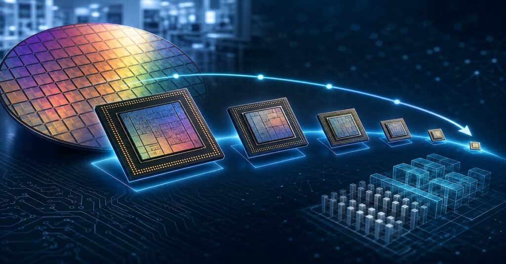
Image Generated With GPT Image 2.0
The End of Scaling as We Knew It
For more than five decades, the semiconductor industry has sustained an extraordinary scaling curve, delivering predictable improvements in computing performance through advances in process technology. Each successive node enabled higher transistor density, greater energy efficiency, and lower cost per transistor, allowing increasingly powerful processors to power everything from personal computers and smartphones to cloud infrastructure and supercomputers. This steady pace of innovation established an expectation that every new generation of semiconductor hardware would deliver substantially more capability than the one before it.
That expectation has become significantly more difficult to maintain. The rapid growth of artificial intelligence has accelerated demand for computational performance at a rate that now exceeds what traditional transistor scaling alone can provide. Training increasingly complex models, processing massive datasets, and supporting real-time inference require dramatic increases in compute density, memory bandwidth, interconnect performance, and energy efficiency. At the same time, semiconductor manufacturers are facing rising fabrication costs, reticle size limitations, higher power densities, increasing thermal challenges, and growing manufacturing complexity. These converging pressures have fundamentally changed what it means to remain on the semiconductor scaling curve.
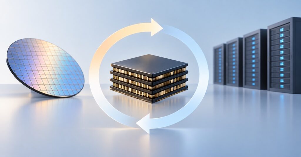
Keeping AI hardware on that trajectory is no longer simply a matter of moving to the next process node. Future performance gains will increasingly depend on advances that extend well beyond transistor scaling, including new processor architectures, heterogeneous integration, advanced packaging, high-bandwidth memory, faster interconnects, intelligent power delivery, and manufacturing innovations that enable these increasingly complex systems to be produced at scale. In other words, the challenge has shifted from scaling a chip to scaling an entire computing platform.
The question facing the semiconductor industry is therefore not whether scaling can continue, but how it can continue. The answer will determine whether future hardware can sustain the exponential growth in computing capability that artificial intelligence and the broader digital economy will demand over the coming decade.
Keeping the Scaling Curve Alive
At the same time, the semiconductor industry has repeatedly demonstrated that innovation does not stop when one technology reaches its practical limits. Instead, it evolves. The transition from planar transistors to FinFETs, from monolithic SoCs to chiplet-based architectures, and from process-centric scaling to system-level co-design illustrates the industry’s ability to redefine how progress is achieved.
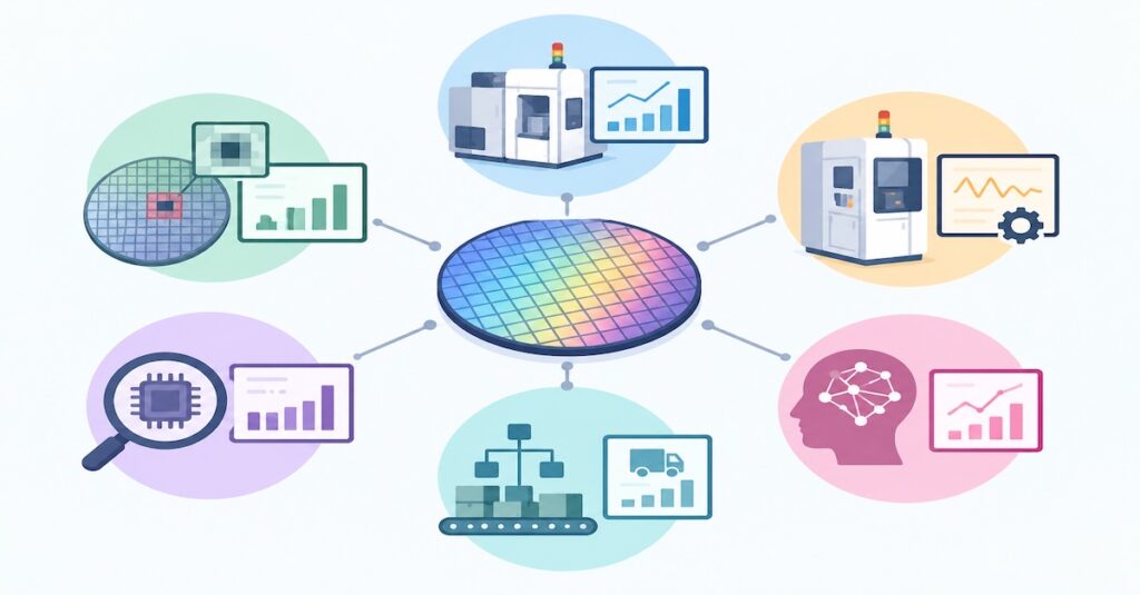
The next phase of semiconductor advancement will similarly depend on combining innovations across architecture, memory, packaging, interconnects, power delivery, manufacturing, testing, and software into a cohesive platform rather than relying on any single breakthrough.
The challenge, however, extends beyond developing new technologies. The industry must deliver these innovations while maintaining acceptable manufacturing yields, controlling costs, improving energy efficiency, and shortening time to market. Success will be measured not only by faster hardware, but also by the ability to manufacture increasingly complex systems reliably and at scale.
Keeping AI hardware on the semiconductor scaling curve will therefore require unprecedented collaboration across the entire semiconductor ecosystem, where progress is determined by how effectively multiple engineering disciplines work together to solve increasingly complex engineering challenges.
| Scaling Driver | Past | Future |
|---|---|---|
| Performance Growth | Process node shrink | System-level co-optimization |
| Compute | Higher clock speeds | Specialized, domain-specific architectures |
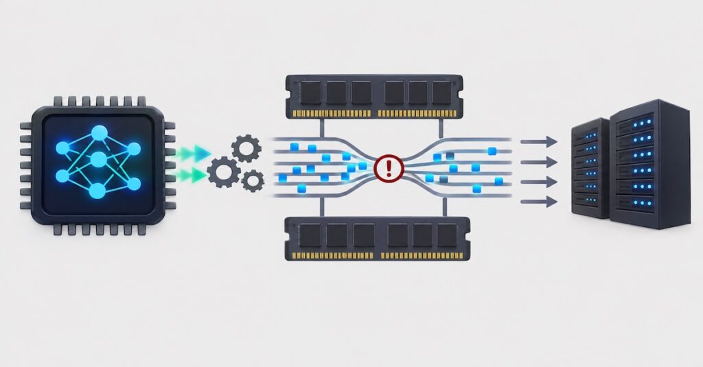
| Memory | Larger on-chip caches | High-bandwidth and disaggregated memory |
| Integration | Monolithic SoCs | Chiplets and heterogeneous integration |
| Connectivity | Conventional electrical I/O | High-speed die-to-die links and optical interconnects |
| Power | Transistor efficiency | Advanced power delivery and energy-aware design |
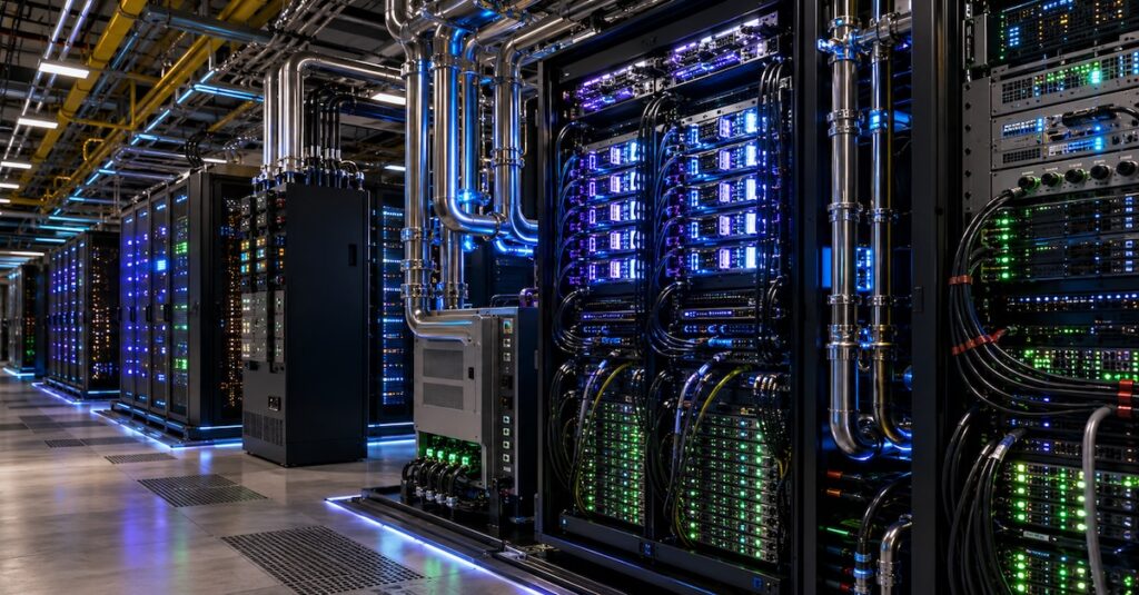
| Thermal | Air-cooled systems | Liquid cooling and package-level thermal engineering |
| Manufacturing | Single-die optimization | Co-optimization across design, packaging, test, and yield |
For more than half a century, transistor density has been the semiconductor industry’s most recognizable measure of progress. As traditional process scaling becomes increasingly constrained by physical and economic realities, that single metric is no longer sufficient to capture the complexity of modern computing systems.
Future hardware will instead be judged by how effectively it integrates advances in architecture, memory, packaging, interconnects, power delivery, thermal management, manufacturing, and software into a cohesive and scalable platform.
Perhaps the next semiconductor scaling curve will not be defined by any one metric at all. Instead, it may be measured by the industry’s ability to simultaneously deliver greater system-level performance, higher performance per watt, increased memory bandwidth, improved manufacturing efficiency, and faster time to market. The challenge is no longer simply fitting more transistors onto a chip.
It is extracting more useful computing capability from an increasingly complex semiconductor ecosystem. If Moore’s Law defined the last five decades of semiconductor innovation, the next era may be defined by how effectively the industry optimizes the entire system rather than any individual technology.
Question: What will define the next semiconductor scaling curve?
Answer: It is unlikely to be a single metric. Instead, it will be defined by the semiconductor industry’s ability to integrate multiple innovations into scalable, manufacturable, energy-efficient, and economically viable computing platforms. The companies that successfully balance architecture, memory, packaging, interconnects, manufacturing, and software will not only keep AI hardware on the semiconductor scaling curve, but also shape the future of computing itself.