
Photo by Stefan Kunze on Unsplash
The semiconductor industry is entering a new era where all high-tech solutions will demand new and advanced semiconductor product-driven solutions. These solutions range from wireless to automotive. In this massive market (upward of $2 Trillion), there will be a need to re-invent different segments within the semiconductor ecosystem.
The products and solutions that will drive a new era of semiconductors will require new (many are already in the market) semiconductor technologies that can provide an edge to different customers. From a technical point of view, this means a perfect combination of an efficient semiconductor design (new FETs) with defect-free semiconductor manufacturing (new Nodes and Packages).
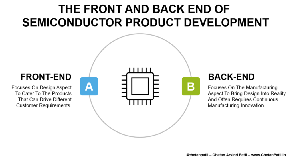
Semiconductor design is the front-end of semiconductor product development, while semiconductor manufacturing is the back-end. These two parts play a crucial role in bringing new solutions to the market.
Front-End: Focuses on design aspect to cater to the products that can drive different customer requirements. It ranges from creating powerful to efficient semiconductor products that enable different types of semiconductor-driven markets like automotive, smartphone, communication, etc.
The major bottlenecks in the front-end development is the research required to bring the solution into reality, and not all efforts eventually get implemented. It also means a long time and investment is needed to push the front-end innovation.
Semiconductor technologies that drive the back-end part (manufacturing) get inspired by front-end innovation. However, there are still several back-end technologies that drive front-end innovation. It is valid mainly for lithography and packages development activities.
Back-End: Focuses on the manufacturing aspect to bring design into reality and often requires continuous push for innovative manufacturing solutions that range from equipment, nodes, packages to materials.
In the end, semiconductor innovation is greatly dependent on the perfect combination of front-end technologies with back-end capabilities. From matured to advanced/new semiconductor technologies, all have been successful due to the features provided by both the front-end and back-end features.
As the semiconductor industry embraces the demand for existing and emerging markets, the importance of creating technical infrastructure for front and back end solutions will grow too. It is why emerging semiconductor destinations need to focus on research and development activities. As it will not only bring new semiconductor solutions into the market but will also train future talents.
Countries that can strike this perfect balance will surely lead the front and back end of semiconductor product development.


