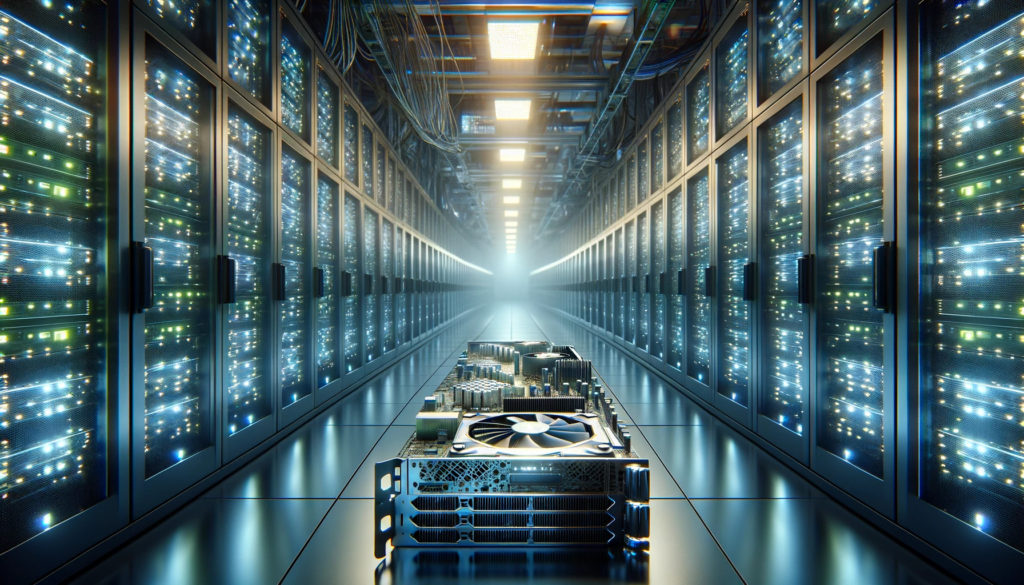
Image Generated Using DALL-E
General Purpose GPU
General Purpose GPUs (GPGPUs) represent a significant evolution in computing, transforming GPUs from specialized hardware focused solely on graphics processing to versatile computing units capable of handling a broad range of tasks. This shift has enabled GPUs to play a crucial role in areas beyond gaming and graphics, including scientific research, data analysis, and artificial intelligence (AI). By leveraging their parallel processing capabilities, GPGPUs can execute complex mathematical and data-intensive operations at speeds vastly superior to traditional CPUs, making them indispensable for tasks requiring high computational throughput.
Traditionally, GPUs are designed and manufactured as monolithic dies, where a single silicon die houses all the GPU’s functionalities. This approach has advantages, such as straightforward design, manufacturing processes, and high-speed internal communication. However, it also faces limitations in scalability, manufacturing yield, and adaptability to rapidly evolving computational demands, especially those driven by artificial intelligence (AI).
AI Specific GPU
As the demand for more versatile and powerful computing resources grows, particularly in AI-driven applications, the semiconductor industry is witnessing the next leap in innovation: the rise of Ghiplet architecture.
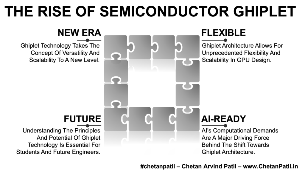
Ghiplet technology takes the concept of versatility and scalability to a new level. By adopting a modular approach, where a GPU gets built from multiple interconnected ghiplets, Ghiplet architecture offers unprecedented flexibility in GPU design. This modularity allows for optimizing specific functions, such as AI computations or memory handling, within individual Ghiplets, which can then be customized to meet the unique requirements of various applications.
Furthermore, the Ghiplet approach addresses some of the critical challenges faced by monolithic designs, such as manufacturing yields and the rapid pace of technological advancement, heralding a new era of GPU technology that is adaptable, efficient, and ready to meet future computing demands.
Ghiplet = G(PU) + Chiplet
Flexible And Scalable
Ghiplet architecture allows for unprecedented flexibility and scalability in GPU design. Depending on an application’s specific needs, different combinations of ghiplets can be assembled to optimize performance, power efficiency, or cost. It starkly contrasts monolithic designs, where changes in functionality or performance often require a complete redesign of the silicon die.
One of the significant challenges with monolithic dies is the lower yield rates associated with manufacturing large and complex silicon pieces. Defects in any part of the die can render the entire chip unusable, increasing waste and cost. Ghiplet architecture mitigates this issue by using smaller, more manageable ghiplets. Since ghiplets are produced separately, a defect in one ghiplet doesn’t necessitate discarding the entire GPU, significantly improving yield rates and reducing production costs.
Data Movement
A crucial aspect of making Ghiplet architecture viable is the development of advanced interconnect technologies. These technologies ensure fast, efficient communication between ghiplets, which is essential for maintaining high performance. Innovations such as silicon photonics and advanced packaging solutions, like 2.5D and 3D stacking, are pivotal.
They enable Ghiplet GPUs to achieve and sometimes surpass, their monolithic counterparts’ communication speeds and bandwidths, overcoming one of the leading technical challenges of modular design.
AI-GPU For AI-Workload
AI’s computational demands are a major driving force behind the shift towards Ghiplet architecture. AI applications require massive data processing, often necessitating specialized hardware accelerators. Ghiplet GPUs can integrate AI-specific ghiplets, offering tailored solutions that are more powerful and energy-efficient than monolithic designs can typically provide.
This adaptability is crucial for staying at the forefront of AI technology development.
Modular Future
The Ghiplet concept represents not just a technological innovation but a paradigm shift in how we think about GPU architecture, especially in the context of AI. Understanding the principles and potential of Ghiplet technology is essential for students and future engineers. It offers insights into the future of computing, where flexibility, efficiency, and specialization become critical drivers of semiconductor design.
As the industry continues to advance, the modular, ghiplet-based approach heralded by Ghiplet technology is set to play a pivotal role in shaping the next generation of computing devices, making it a critical area of study and exploration for anyone interested in cutting-edge semiconductor technology.


