
Photo by Patrick Lindenberg on Unsplash
THE REASONS TO ADOPT IN-MEMORY SEMICONDUCTOR PROCESSING
Over the last decades, both industry and academia have spent numerous hours to enable different types of semiconductor design and manufacturing methodology to drive next-gen processing units. These processing units today power the computing world and often require billions of ever-shrinking structures.
As the data world moves towards more complex workloads coupled with the need for faster and real-time processing, the traditional processing units will not be enough for the computing task. To overcome challenges, the semiconductor industry (mainly companies focused on XPUs) is now adopting new semiconductor design and manufacturing methods for processing units. Chiplets is one such example.
In-Memory Processing Combines The Memory Units And Processing Units Into One Single Block And Thus Enabling Faster
However, the problem chiplets solves is the technology-node wall, and thus enable the future demand of a more efficient system without compromising the shrinking transistor size. In the long run, chiplets may not solve the memory bottleneck, as it occurs due to the need to bring the data from the lower level memory to memory closer to the processing units. All this leads to traffic and thus architecture-level bottlenecks.
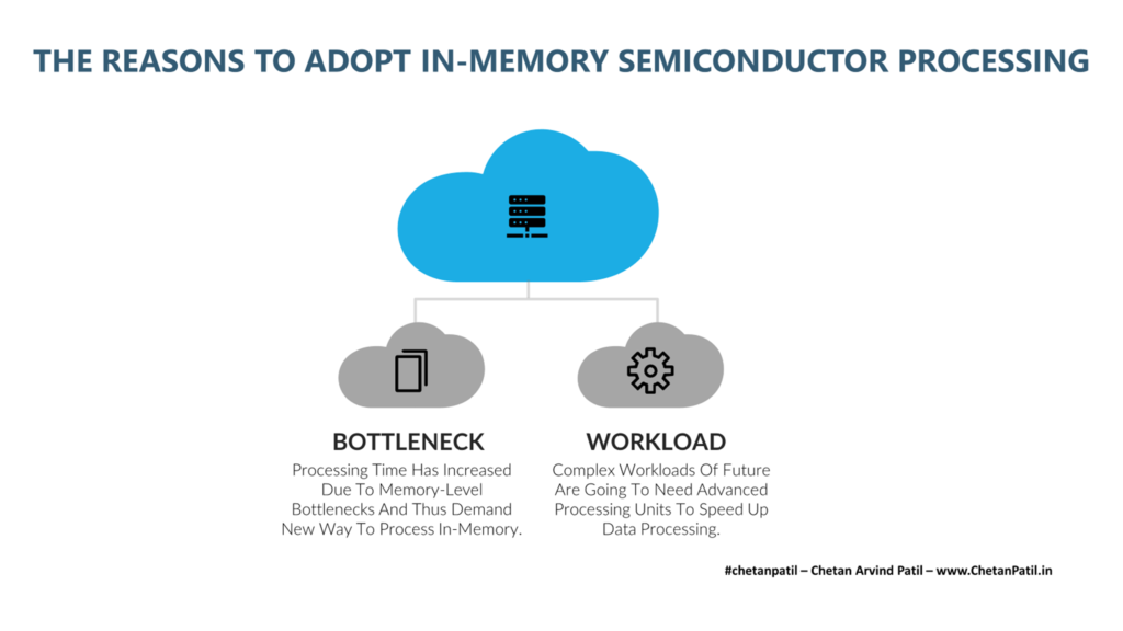
Bottleneck: The time required to bring the data from lower-level memory to high-level memory (closer to the processing units) adds a time-related penalty and leads to a bottleneck when a given XPU has many processing units. Memory and compute level bottlenecks are thus demanding new processing solutions, and in-memory processing could be one such solution.
Workload: Workloads today demand video to audio to text to graphics-related processing. Traditional XPU design can handle these but again require different dedicated processing units for specific processing requests. NPU for neural, CPU for computing, DSP for digital, and so on. Specific purpose processing units add complexity. Thus, an in-memory processing unit solution can provide a foundation to minimize the block-level complexity and thus enable faster workload processing by bringing computing to the core of memory units.
Designing and fabricating different computing units can unlock new features that can speed up the computing world for future workloads. There are several challenges and hurdles in bringing this to reality. However, if done correctly, then the impact is only positive. In the long run and how the computing world is changing year on year, In-Memory processing is a path forward for data-heavy systems like server-grade XPUs.
THE HURDLES TO ADOPT IN-MEMORY SEMICONDUCTOR PROCESSING
In-Memory processing units are a promising solution to tackle both the XPU bottleneck and the demand to handle complex workloads. Both academia and industry have proposed several solutions with many in-memory processing units ideas already tried and tested.
However, using in-memory processing units at the server level (where this solution finds the perfect fit) is still a far distant dream. The two critical hurdles stopping the large-scale adoption of in-memory processing units, and both of these go hand in hand.
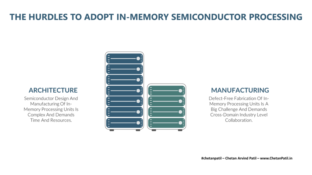
Architecture: Combining processing units and memory units into a single unit (manufactured together) demands thorough research and design. It takes resources, cost, and time to do so before a viable product gets released. While it is not impossible to come up with a working mass-market in-memory processing unit solution, the time taken and risk involved is too high, something only a selected few companies in the market are capable of doing so.
Manufacturing: After semiconductor design, the semiconductor manufacturing stage is critical in fabricating two different units into one. In-Memory processing units demand combining two separate semiconductor manufacturing worlds. Doing so requires semiconductor design, semiconductor FAB, and also semiconductor equipment manufacturers to come together.
XPUs for the throughput-oriented requirement will keep evolving. Yesterday it was CPU and GPU, today ASIC/FPGA, and tomorrow it could be In-Memory processing units. In the end, as long as the solution is feasible from both the design and manufacturing point of view, the market will embrace it.
Several emerging companies are already coming up with new architectures to design next-gen XPUs. In-Memory processing units will also go similar traction, and it will be interesting to see how the market will behave.


