
Photo by Mayer Tawfik on Unsplash
It has been one year since the US passed the CHIPS And Science Act. Ever since then, the American semiconductor ecosystem has seen a lot of activities and ground progress.
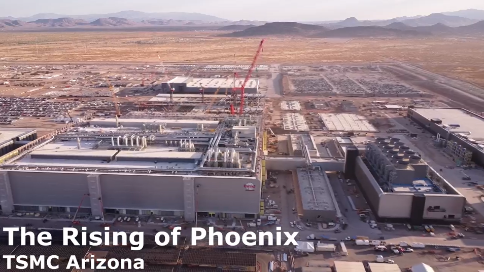
It is evident from the expansion of Intel’s network of FABs in the US and the almost complete 5nm ultra-advanced node (subsequently 3nm) FAB21 of TSMC in Phoenix, Arizona. The CHIPS And Science Act has also re-energized the semiconductor ecosystem in Texas, where Samsung is creating a new semiconductor cluster in the City of Taylor, Texas. Similarly, Micron Technologies, GlobalFoundries, Texas Instruments, SkyWater, and many other semiconductor Pure Play and IDMs have planned new semiconductor manufacturing plants.
It is not only the semiconductor manufacturing part of the supply chain that the CHIPS And Science Act has touched. This act has rightly focused on several other critical parts of the semiconductor ecosystem, including new semiconductor-focused university programs, research funds, and workforce reskilling.
For a semiconductor ecosystem to thrive in any country, the focus must be on these critical pillars (Academia, Research, Workforce, Infrastructure), and the CHIPS And Science Act has started to impact all of these.
Academia:
Progress of semiconductor technologies is highly dependent on the workforce, and this act has provision to invest in training and research activities around semiconductor education.
For example, it has helped Arizona State University work with industry to create the correct set of future workforce and has also developed a certification program for students and professionals.
The act has helped Purdue University offer a range of semiconductor and microelectronics-focused courses and exclusive degree programs, including collaboration with upcoming international regions like India.
Similarly, several other universities have started structuring programs focusing mainly on semiconductors.
Research:
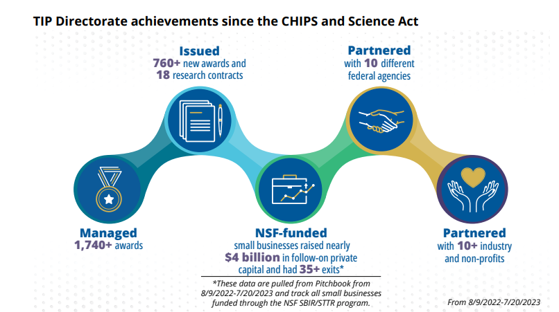
The impact of the CHIPS and Science Act has started showing up in the form of an increase in research activities by the National Science Foundation (NSF).
NSF has already awarded numerous contracts and funds to spearhead the semiconductor research, now helping universities, faculties, and graduate students focus on the much-needed research solutions on the process node to physics that make up the semiconductor EUV equipment. All of which will feed into the US’s existing and upcoming semiconductor manufacturing facilities.
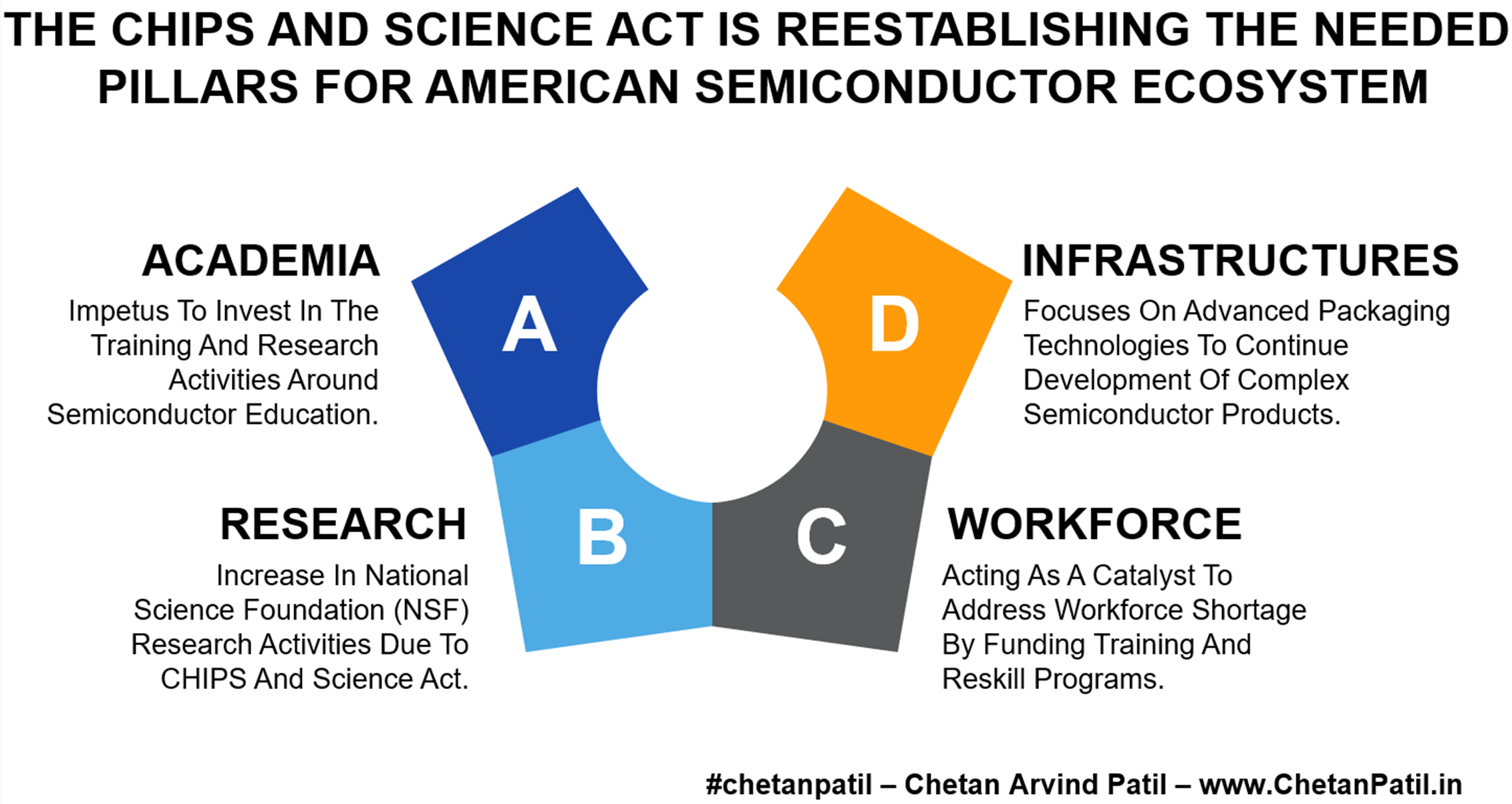
Workforce:
With the recent shortage of semiconductor workforce, the CHIPS And Science Act has rightly set the focus on this front, and that too at the much needed time.
For example, Purdue University has started the Summer Training, Awareness, and Readiness for Semiconductors (STARS) program—an eight-week course to develop skills in fabrication, packaging, and semiconductor device and materials characterization.
Similarly, The First Virtual Cleanroom Environment for Semiconductor Manufacturing Technology was released to help professionals re-train themselves (or new workforce) to align with the advancing fabrication process. It is also slowly becoming a valuable tool to train the new fab workforce.
Infrastructures:
Apart from the existing push from the private semiconductor FAB players, the CHIPS And Science Acts also focus on futuristic and advanced packaging technologies, which are the core of semiconductor product development.
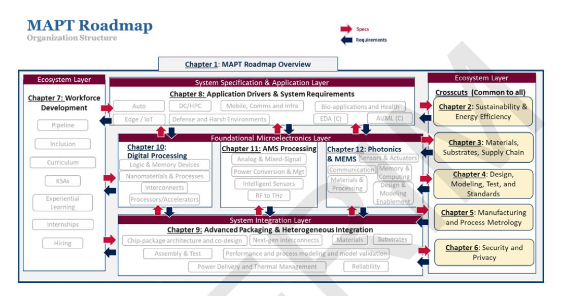
In a similar line, the National Institute for Standards and Technology (NIST) has set a clear focus on establishing the National Semiconductor Technology Center (NSTC) and National Advanced Packaging Manufacturing Program (NAPMP) that will enable America’s ability to develop the chips and technologies of the future to safeguard America’s global innovation leadership.
The Microelectronics and Advanced Packaging Technologies Roadmap (MAPT) shows how NIST (in collaboration with SRC) will focus on advancing back-end semiconductor manufacturing innovation.
Within one year, the CHIPS And Science Act has helped the semiconductor ecosystem in the US to focus on the much-needed pillars of semiconductor-focused academic programs, research, workforce, and infrastructures.
More results will be seen in a few years when new FABs, Assembly, And Testing facilities are operational and have access to the trained workforce.
So far, the vision of re-establishing the end-to-end semiconductor supply chain in the US is on track, eventually bringing in new waves of semiconductor-driven innovation and growth.


