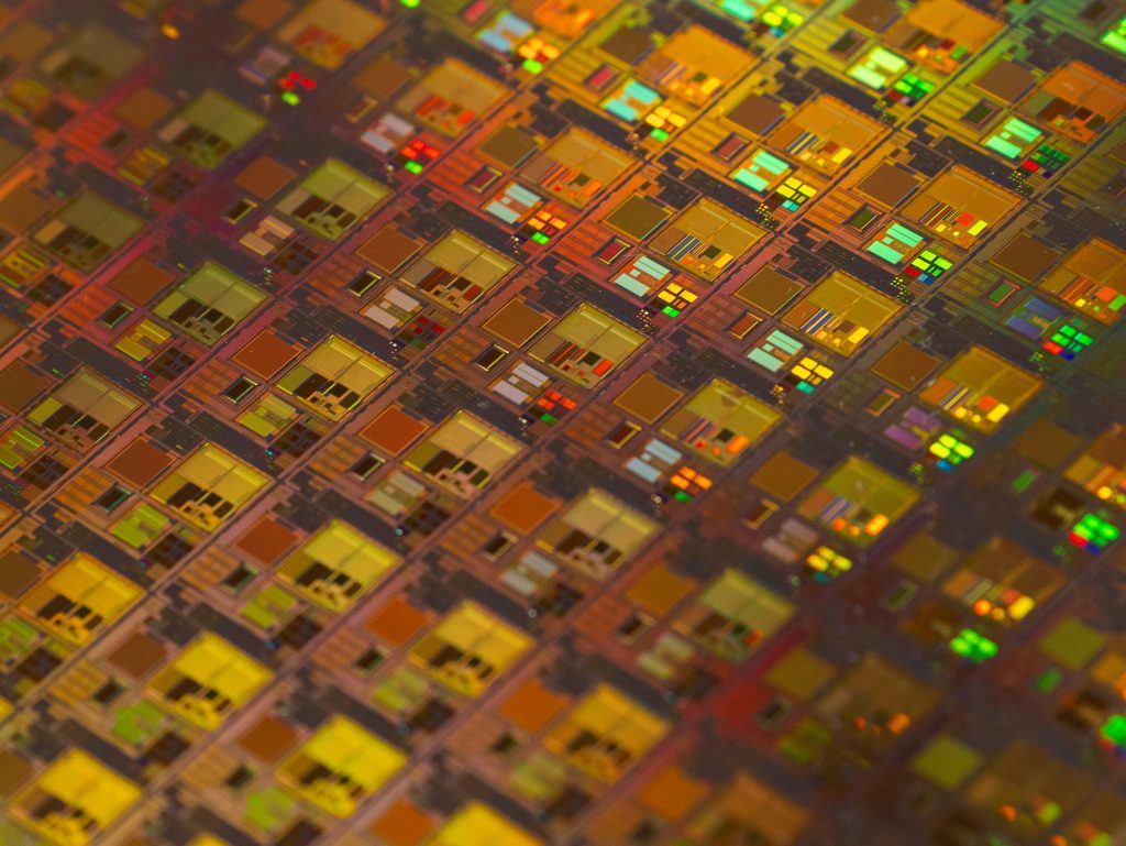
Photo by Maxence Pira on Unsplash
These latest trends in semiconductor manufacturing are significantly impacting the industry. These trends lead to faster, more powerful, and more efficient semiconductor chips. It drives demand for semiconductors in various applications, from smartphones and computers to cars and medical devices.
Thus, it is critical to see the most impactful changes occurring in the semiconductor manufacturing arena. As an example, the following technical trends are changing the future course of semiconductor manufacturing:
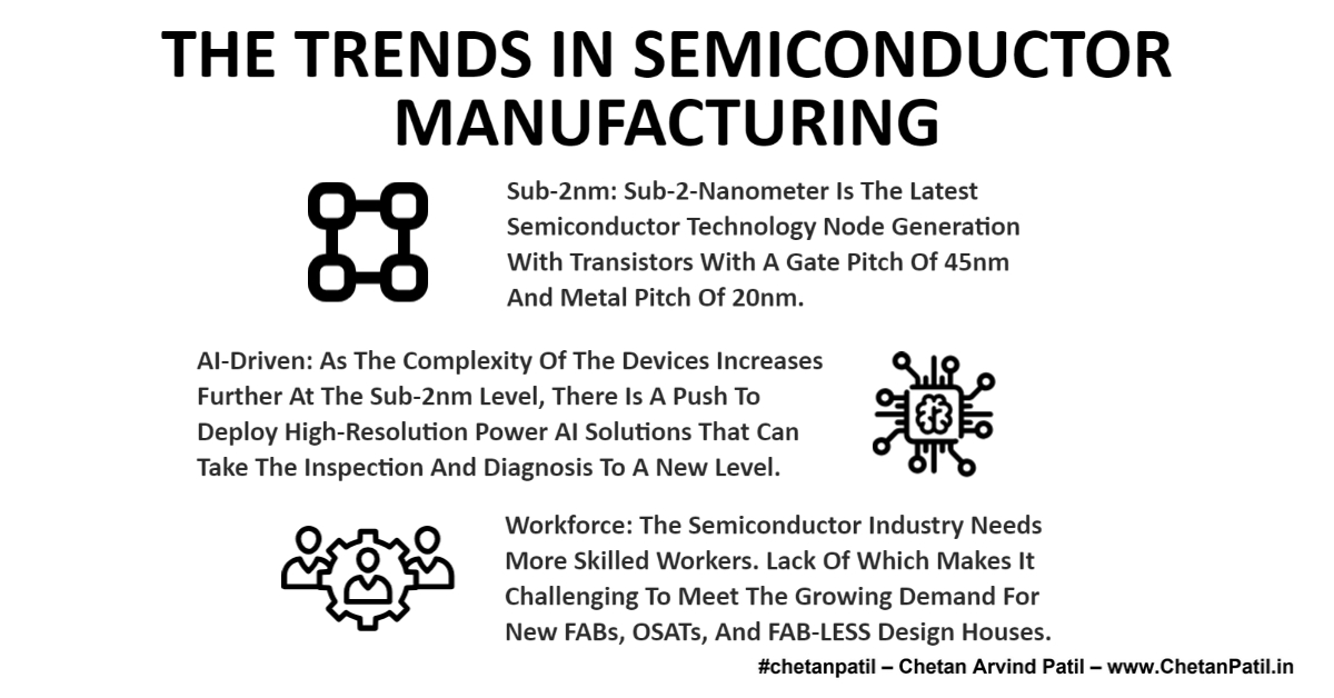
Sub-2nm: Sub-2-nanometer is the latest semiconductor technology node generation with transistors with a gate pitch of 45nm and metal pitch of 20nm. Depending upon the semiconductor manufacturer, different types of new FET devices will be available at 2nm. Examples: MBCFET, GAAFET, and RibbonFET. Such narrow processes and optimized devices allow more transistors to get packed onto a single chip, which can lead to significant performance improvements.
Vertical Packing: Continuous rise of 3D stacking to allow stacking of multiple chips. It continues to increase performance and density significantly. Slowly it is becoming more cost-friendly, thus opening avenues for broader use cases.
Materials: Advanced materials are getting developed that can improve the performance and efficiency of semiconductors. For example, new high-k dielectric materials are to replace the traditional silicon dioxide used in gate insulators. These new materials can improve the performance of transistors by reducing leakage current and allowing for smaller transistor dimensions.
Workforce: The semiconductor industry needs more skilled workers. Lack of which makes it challenging to meet the growing demand for new FABs, OSATs, and FAB-LESS design houses.
Having a right set of technical trends that encompasses several aspects of showcases where the semiconductor industry is heading and also how it can utilizes these changes to better blend the next-gen devices.
On the core equipment and tooling side, significant changes are also about to come. Some of these are listed below. However, the cost of manufacturing associated with these will also have a considerable impact.
xUV: Sub-2nm node is leading to a new type of lithograph equipment. ASML is the leader and targets two types of lithography machines for the market: the 2nm EUV and the 1nm EUV models. The precision of the devices depends on their NA (Numerical Aperture) value. The NA value for the 2nm and 1nm machines is 0.55, while the NXE 3400C has a NA value 0.33. With such High-NA lithography, ASML and other semiconductor equipment developers are about to disrupt the semiconductor processing node.
Chiplets: The way designing an SoC with multiple chiplet is setting new standards for the chip designers and the tools used for it; the manufacturing aspect of it is also changing as it requires managing multiple manufacturing flows and then bringing it all together to drive the next-gen application level system solution.
AI-Driven: As the complexity of the devices increases further at the Sub-2nm level, there is a push to deploy high-resolution power AI solutions that can take the inspection and diagnosis to a new level, thus enabling high yield, improved performance, and reduced time to market. On the design front, the EDA tool vendor is already deploying solutions leveraging AI to allow chip designers to faster process movement from the previous generation to the future age of nodes.
Cost: The cost of semiconductor manufacturing is always on the rise. It is leading to low margins. Increasing cost also makes it difficult for the new manufacturing houses to drive faster returns on investment.
These are only a few of the trends that are shaping the semiconductor manufacturing industry. As the semiconductor industry continues to evolve, it will be interesting to see how these trends play out and what new developments emerge in the years to come.


