
Image Generated Using DALL-E
Students And Computational Lithography
I recently wrote about computational lithography. Several students asked, apart from mathematics skills, what more is required to align educational training so one has a better chance of joining semiconductors as a computational lithography engineer.
I thought a lot about this, and outlined in this blog are all the ins and outs of computational lithography that can benefit students.
What Is Computational Lithography
Computational lithography, a critical component of the semiconductor manufacturing process, represents the intersection of computer science, physics, and engineering, tailored to enhance the capabilities of photolithography. Photolithography is a process used to transfer geometric patterns onto a substrate or silicon wafer, essential for creating the intricate circuits that form the backbone of electronic devices.
The field of computational lithography encompasses advanced algorithms and software tools to optimize this patterning process. Given the physical limitations of traditional lithography techniques, particularly as the semiconductor industry strives to shrink chip features to the sub-nanometer scale, computational lithography emerges as a pivotal solution. It enables the production of smaller, more efficient, and powerful microchips beyond the constraints of optical lithography.

Why Learn About Computational Lithography
Learning computational lithography is becoming increasingly critical, especially within the semiconductor industry’s relentless drive toward miniaturization and efficiency improvement.
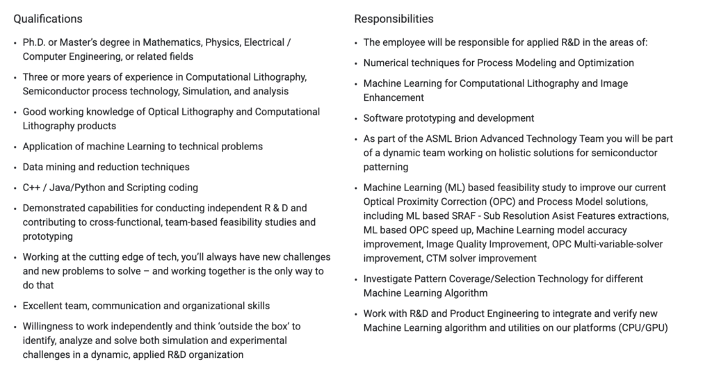
Several vital roles demand skills in computational lithography. Below is an example of a job description requiring computational lithography skills:
If as a student you are looking for more critical and technical reasons on why learning computational lithography is invaluable. Then below is a guide that can helpful.
| REASONS | DESCRIPTION |
|---|---|
| Central Role In Semiconductor Manufacturing | Essential for producing advanced semiconductor devices, enabling continued technological advancement. |
| Addressing Physical Limitations | Provides solutions to surpass the physical limits of traditional lithography, enabling the creation of nanoscale features. |
| High Demand For Skilled Professionals | Expertise in computational lithography is highly sought after, with growing demand as technology evolves. |
| Interdisciplinary Skill Development | Fosters a wide range of skills from various disciplines, valuable across the semiconductor industry and beyond. |
| Enabling Advanced Technologies | Key to the development of cutting-edge technologies for advanced to ultra-advanced chips |
| Research And Development Opportunities | Numerous opportunities for contributing to new techniques and methodologies in lithography. |
| Economic And Strategic Importance | Contributes to the strength of the semiconductor industry, a cornerstone of the global economy and national security. |
| Personal And Professional Growth | The evolving nature of computational lithography encourages lifelong learning and adaptability. |
| Collaborative And Multidisciplinary Work Environment | Involves working in collaborative, multidisciplinary teams, fostering innovation and problem-solving. |
| Global Network And Community | Engaging with computational lithography opens doors to a global community of experts and industry leaders. |
How To Learn And Enhance Skills Around Computational Lithography
Learning and enhancing skills in computational lithography involves a multidisciplinary approach, blending principles from physics, engineering, computer science, and mathematics. This field is crucial for those aspiring to contribute to the semiconductor industry’s evolution, particularly in designing and manufacturing ever-smaller and more efficient microchips.
Here’s a structured pathway to learn and enhance your skills in computational lithography:
| STRATEGY | DESCRIPTION |
|---|---|
| Solidify Your Foundation In Physics And Mathematics | Focus on optics, quantum mechanics, electromagnetism, calculus, differential equations, linear algebra, and numerical methods. |
| Gain A Deep Understanding of Semiconductor Fabrication Processes | Learn the basics of semiconductor manufacturing and specialize in lithography processes. |
| Develop Computational Skills | Gain proficiency in programming languages (Python, MATLAB, C++) and familiarize yourself with software tools for simulation and design. |
| Engage In Hands-On Projects And Simulations | Work on practical projects or simulations, and participate in team projects to apply theoretical knowledge. |
| Stay Updated With The Latest Research And Developments | Read journals, attend conferences, and participate in workshops to stay informed about the latest advancements. |
| Pursue Advanced Education | Consider specialized courses, certifications, and advanced degrees focused on lithography and semiconductor manufacturing. |
| Network With Professionals And Join Communities | Connect with experts through professional networks and online communities focused on computational lithography. |
| Learn From Industry Experience | Seek internships or co-op opportunities in semiconductor manufacturing companies or research institutions. |
| Critical Thinking And Problem-Solving Skills | Participate in challenges or competitions and study case studies to enhance problem-solving skills. |
| Adopt A Lifelong Learning Mindset | Embrace continuous learning to keep up with the evolving field of computational lithography. |
Take Away
As students navigate the ever-evolving landscape of semiconductor technology and innovation, embracing the field of computational lithography offers a unique and rewarding pathway to making significant contributions to the semiconductor industry and beyond.
This discipline, lying at the intersection of physics, mathematics, engineering, and computer science, not only challenges you to apply and expand your academic knowledge but also positions you at the forefront of technological advancements that power our modern world.
By diving into computational lithography, students will prepare for a career that has the potential to open doors to becoming part of a global community of innovators, researchers, and professionals who are driving the next wave of the semiconductor technological revolution.


