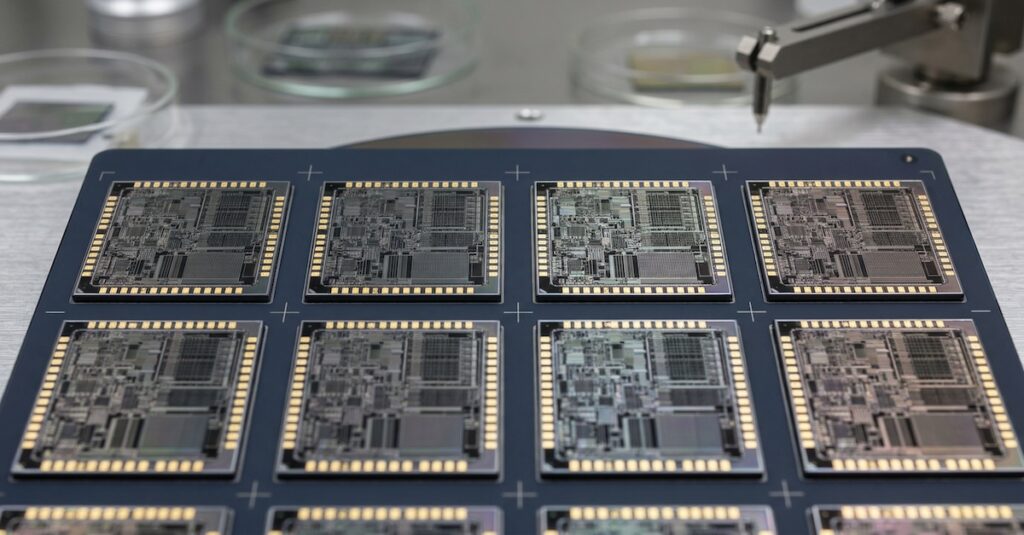
Image Generated Using Adobe Firefly
Semiconductor test engineering is a specialized domain within the semiconductor industry that ensures integrated circuits (ICs) function correctly and meet industry standards before delivery.
The progression from matured nodes (above 40nm) to advanced nodes (at and below 40nm) has brought about profound changes in the domain of test engineering.
As an example:
Coverage: Ensuring complete test coverage becomes challenging as node sizes shrink and transistor counts increase. Test engineers must develop strategies to cover more potential defect sites without increasing test time and, thus, the cost, which is challenging.
Variations: Advanced nodes are more susceptible to process variations. It emphasizes testing for parametric variations to ensure every chip meets performance and power specifications. It requires collecting quality data during fabrication and ensuring all defective parts get captured during fabrication or testing. All of this adds to the productization cost.
Defect Mechanisms: As nodes have scaled down, new defect mechanisms related to manufacturing, like random defects and systematic variation, have emerged, requiring new test methodologies. It has increased the cost of capturing these as more sophisticated data and inspection software tools are needed.
Power: Advanced nodes have power management techniques like multiple power domains, dynamic voltage scaling, and other state machine-driven power requirements. Testing such features requires specialized test patterns and methodologies. Doing so means investing in ATE configurations that can provide the needed setup.
The dense transistor count on newer nodes made achieving comprehensive test coverage more difficult. Moreover, these advanced nodes have vulnerability to process variations, demanding rigorous testing to ensure consistent performance and power metrics.

The evolution of semiconductor nodes also means complexity in Design for Testability (DFT) has risen, with advanced nodes demanding refined techniques to cater to innovations like 3D stacked ICs and necessitating through-silicon via (TSV) tests. Concurrently, methods such as logic built-in self-test (LBIST) and memory built-in self-test (MBIST) have undergone significant transformations.
DFT (Design for Testability) Complexity: As nodes have advanced, DFT techniques have become more sophisticated. They are demanding more test hooks to enable coverage.
Cost Considerations: The cost of testing has been rising, especially for advanced nodes, due to the need to use high-cost ATE systems. It has led to a focus on reducing test times without compromising coverage and adopting more concurrent testing strategies.
Reliability Testing: With the proliferation of devices in critical applications (e.g., medical, automotive), there is an increased emphasis on testing for reliability, longevity, and resistance to conditions like high temperature and radiation. As more transistors get packed in the smallest area possible, test escapes are always possible, which can lead to quality concerns.
Data and Machine Learning: With the vast amount of data generated during testing, there is an increased emphasis on using machine learning algorithms to predict defects, optimize test sequences, and improve yield. It is more valid at matured nodes due to the wafer size and the need to develop cost-mitigation techniques to reduce the need to redo a similar process with a test program.
As the semiconductor industry moved from matured to advanced nodes, test engineering has evolved from focusing on basic functionality checks to a comprehensive discipline that ensures performance, power efficiency, reliability, and safety across intricate designs and multifaceted applications. It invited the problem of cost and time to market and, in many cases, made the productization more complex than ever.
This story is bound to continue with chiplets, ultra-advanced, and other More-Than-Moore methodologies.


