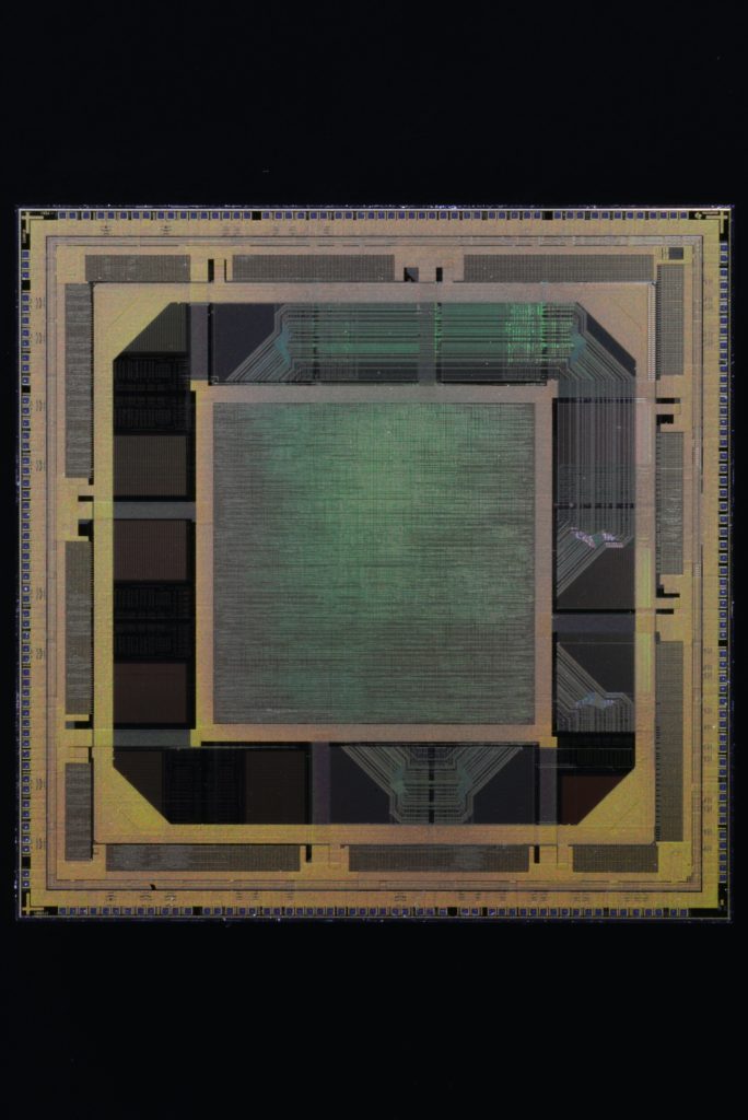
Photo by Laura Ockel on Unsplash
Chiplet is undoubtedly the most suitable semiconductor design and manufacturing solution to scale complex chips reaching the reticle limit. Several silicon products have already adopted chiplet, mainly processors. These products have showcased that using multiple chiplet can significantly improve performance. All while not worrying about the reticle or device constraints.
Several initiatives have come up to speed up the adoption rate of chiplet. Like, Universal Chiplet Interconnect Express (UCIe), which is an open specification for bridging different types of chiplets from the same or multiple vendors by standardizing the interconnectivity, quality, reliability, and several other aspects that are critical to a chip build using the disaggregated approach. Similarly, a few more industry and academia consortiums have emerged, focusing on several criteria to ramp up mass chiplet adoption.
Even with all these steps, certain fundamental hurdles remain, and careful planning is needed before any company uses chiplets to develop silicon chips.
Wafer management is one such hurdle. As the number of chiplets per silicon design increases, so will the number of wafers, adding cost to the already costly process.
Wafer Management:
– A chip designed using chiplets methodology will consist of multiple wafers, with each wafer focused on producing a specific silicon chiplet
– As an example, an XPU with N chiplets will require N number of wafers, and thus, as many wafer management flows
– Merging these N wafers into a single package via heterogeneous integration is going to be complex, time-sensitive, and prone to errors
– Apart from this, the fabricating, testing, and assembly process of each of these wafers will add extra cost that may be more than the aggregated approach
With each wafer comes the challenge of achieving the reference yield.
Yield:
– Chiplets with less complex designs (due to the splitting of larger die areas into multiple chiplets) will still have to go through the required yield check process
– The more the number of chiplets, the more time intensive the yield check becomes (multiple data sources)
– The hurdle here is also to manage the specifications
– So far, the best possible way to mitigate this would be to consolidate the larger block into a single chiplet and repeat the same with other blocks of a larger silicon chip
– Even then, the questions of managing and achieving the yield remain, and multiple-chiplet only adds to the already complicated flow
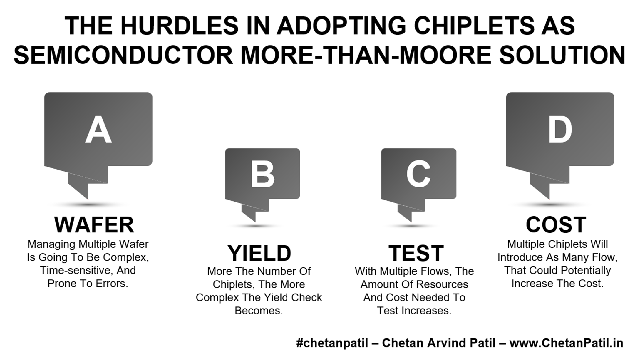
Efficient testing of chiplet is another hurdle.
Test:
– Every chiplet will have a unique wafer, and if multiple such wafers are consolidated to create an end silicon chip, testing is crucial and, by default, part of the process flow
– With multiple flows, the amount of effort needed to test increases.
– It leads to more resources and testing hardware
– Eventually, adding to the testing cost
– If this is more than the cost of testing an aggregated chip, the industry must develop a process to optimize it
To turn multiple chiplets into working silicon chips is also about managing overall development costs. Today, the cost of chiplet will be higher than the aggregated approach due to increased resources required by the multiple chiplets.
Cost:
– Fabricating, testing, and assembly cost is increasing with the increase in the test complexities
– When working with chiplets, managing the expense to prevent higher costs of working with multiple wafers (each wafer = chiplet) is crucial. Otherwise, it will not seen as a valid alternative aggregated flow
– Chiplet should be seen as a More-Than-Moore solution but also as a cost-optimization solution
– Eventually, the goal is also to manage the increased cost of designing chips as large as a reticle (26 mm by 33 mm)
– Lastly, the human resources required for chiplet will be more than needed for an aggregated approach. Which will add to the cost too
No doubt, chiplets have the potential to address several aggregated technical and business challenges. However, the chiplets will be limited to certain types of silicon chips, like XPUs.
For chiplets to be disruptive, mentioned manufacturing flow-driven challenges should be resolved. Otherwise, the journey towards and beyond sub-1nm will be more aggregated than disaggregated.


