THE NEED OF ADVANCED SEMICONDUCTOR EQUIPMENT
High-Tech manufacturing is not possible without the use of equipment. The equipment ensures that the product being manufactured is defect-free and also meets the quality requirement for the target market.
The same fundamentals apply to the semiconductor industry, where equipment plays an important role. Given the need to fabricate semiconductor products without even touching the wafer/die area, requires equipment that can do the task and that too without adding delay or defects.
Every stage of the semiconductor product development requires high-tech equipment, that is why semiconductor fabrication, testing, and assembly facility is 90% occupied by the equipment. These advanced equipment require only a set of commands (called recipes) to complete the task they are assigned. The automation achieved with this process ensures the FAB/OSAT are running at full capacity 24x7x365. This is why it is often a challenge for the semiconductor FAB and OSAT to ensure the equipment never goes down and this requires periodic maintenance that is often driven by data collection and analysis.
Semiconductor FAB and OSAT often have two different types of equipment:
Advanced: Advanced equipment is often robotic driven. This includes moving the wafers and other materials (mainly reticle). Apart from robotic capabilities, advanced equipment often has data capturing capability that is then stored for further wafer/die analysis.
Non-Advanced: These types of equipment in the semiconductor process are confined to analysis or lot transferring, and do not have the robotic capability and are more useful for manual inspection or testing.
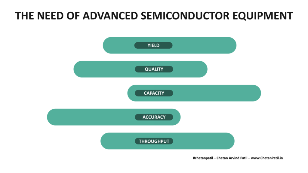
Majority of the equipment in the semiconductor FAB/OSAT are advanced and are designed for the following goals:
Yield: Primary target of any semiconductor FAB/OSAT to ensure there is minimal to zero yield loss. This is only possible if the process of handling and using materials (reticle, wafer, etc.) adheres to the standards that ensure high-yield. This is where equipment come into the pictures, and the materials are handled and processed in a manner that does not negatively affect the semiconductor wafer, thus ensuring minimal yield loss.
Quality: Quality is the primary de-facto target of every semiconductor product. Equipment can be handy to capture any issues/variations/excursion during the semiconductor process. Whether it is during the lithography stage or automated inspection, equipment ensures the process being executed is eventually leading to correct wafer/die formation.
Capacity: The primary target of FAB/OSAT is to ensure the facility is 100% utilized. This is only possible if there is an advanced equipment that is working non-stop day in and day out. Without investing in the equipment to increase efficiency, it is not possible to utilize FAB/OSAT fully.
Accuracy: Advanced equipment is also important from an accuracy point of view. They ensure the target design is fabricated without any gaps. From etching to deposition to even assembly, accuracy/alignment can only be achieved if the equipment is used. If the manual process is used, then it will not only lead to errors but also bring the FAB/OSAT capacity down.
Throughput: Semiconductor products get utilized by different industries and markets. To timely provide them with the products requires high efficiency. This is made possible by advanced equipment that can process wafers after wafers to keep up with the demand. On top of this, any given FAB has numerous parallel equipment doing the batch processing, thus ensuring the throughput is always at the maximum level possible.
The semiconductor FAB/OSAT are utilizing advanced equipment to keep the facility running that eventually drives revenue. However, ever changing technology-node and device structure is also putting pressure on the FAB/OSAT to upgrade their equipment often.
While the majority of the advanced equipment has a plug-and-play feature for easy upgrades, CapEx and maintenance teams are required to keep the equipment running which in turn runs the FAB/OSAT.
Irrespective of the features or the CapEx hurdles, advanced semiconductor equipment is vital for high-quality semiconductor product development.
THE TWO SIDES OF ADVANCED SEMICONDUCTOR EQUIPMENT
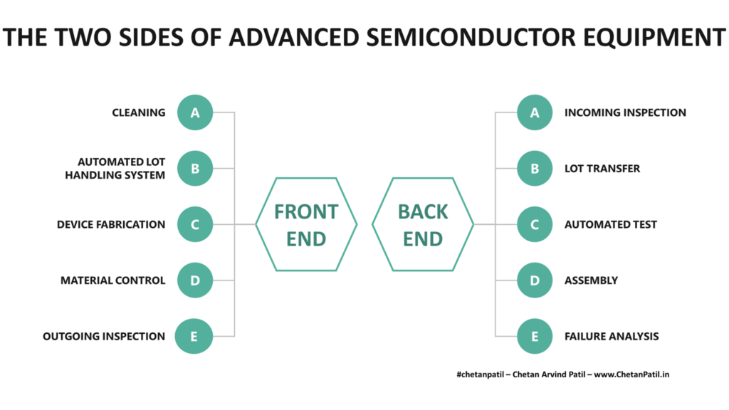
There are different types of advanced semiconductor equipment that are used by the FAB/OSAT. They often get categorized based on which part of the wafer fabrication the equipment is used for.
Front-End: The advanced equipment for the Front-End process is used in a semiconductor FAB. There are different advanced equipment that does the task as per the process flow they are part of.
Cleaning: This process utilizes equipment to clean wafers/lots post a wafer stage. Whether cleaning is required or not depends on the recipe that semiconductor engineers design for a given product based on its features and requirements.
Device Fabrication: This stage (the most critical one) requires different equipment to carry out different device fabrication steps from lithography to etching to interconnection to diffusion. Using equipment for device fabrication, the end goal of the wafer with dies having FETs is achieved.
Automated Material Handling: This is the most vital part of the process where the equipment is used to deliver a lot (using FOUP) from one section of the FAB to another. The equipment to do this task eventually forms a semiconductor highway inside the FAB, which autonomous vehicles use to retrieve/deliver lots from one stage to another.
Material Control: Equipment used for this process is focused on controlling the materials like chemicals etc., to ensure the equipment/process needing it like it when required. It is vital to ensure it is done with proper safety, otherwise, a small leakage can cause an emergency.
Outgoing Inspection: The last stage of the wafer fabrication is often to ensure the outgoing lot (for the OSAT), is defect-free. This requires the usage of highly automated robotic inspection equipment that ensures any defect is captured (reported too) and the final wafer map is generated accordingly.
After the wafers have been shipped out of the FAB, the next stop is OSAT. Which requires different (some similar) equipment to drive the semiconductor process.
Back-End: The advanced equipment used for the Back-End process is designed for OSAT.
Incoming Inspection: Equipment to perform incoming inspection is similar to the one used for outgoing inspection. The goal is to remove any die defect that occurred during the shipping process. Inspection equipment is high on speed and the data generated is analyzed and stored for the future use.
Lot Transfer: The shipping box that arrives at OSAT eventually has to get transferred to a different FOUP. This is where equipment comes in handy that can take all the wafers in the lot and transfer it to another FOUP without human intervention. This ensures there are no particles or human errors. Tracking is done via lot/wafer id.
Automated Test: Automated Test Equipment (ATE) is loaded with the wafer (along with the probe hardware) and then a test program runs on every die of the wafer. The test is required to capture electrical characteristics, which is part of the process to ensure the defective die (root cause can be many) are not processed further.
Assembly: Depending on the assembly recipe, the equipment takes the wafer and assembles the parts. This stage can involve bumping to dicing. Each of which requires its own set of equipment. This process certainly cannot be done by humans and hence advanced equipment is a must.
Failure Analysis: Eventually, if multiple materials have set failing patterns, then failure analysis needs to be carried out. The advanced equipment required for failure analysis often has biasing capability apart from features to dive inside the die at the gate level with the help of highly advanced X-Ray techniques.
Both FAB and OSAT are heavy equipment driven facilities. While there are opportunities for the equipment industry to enable new solutions, at the same time it requires a balance of equipment features and the usage cost.
THE OPPORTUNITIES FOR ADVANCED SEMICONDUCTOR EQUIPMENT
The advanced semiconductor equipment market is poised to grow mainly due to the race to set up new FAB and OSAT by countries wanting to establish the lead in the semiconductor industry. This certainly presents opportunities for advanced semiconductor equipment manufacturers.
However, given that the semiconductor equipment market itself is highly competitive, the new equipment solutions need to focus more on features that can make the equipment stand apart in the market.
There are many features/areas that advanced equipment manufacturers can explore apart from the following two:
Automation: While the semiconductor equipment is already highly advanced and automated, there are still parts that can be automated. This might be from materials handling to/from the equipment. Maybe a more data-driven approach to finding how to optimize the lot handling process.
Data: Capturing more data and analyzing it to focus on the equipment wellbeing. This can be from understanding maintenance requirements to predicting when the machine can breakdown. Any predictive information can aid in balancing the cost and productivity by ensuring equipment are up and running all the time.
The top players providing advanced semiconductor equipment solutions are increasing market share every year. This is putting pressure on small scale equipment makers that are trying to competing against these top players. Given the increasing focuses on the semiconductor industry due to the shortage, it is about time the equipment makers (small scale enterprise) take note of the gaps and provide solutions.
Apart from the new equipment market, the used marketplace is also getting a lot of traction. Emerging companies are now providing FAB/OSAT with the opportunities to tap into the low-cost equipment that is not new but certainly can provide the same defect-free features/processing as the new ones.
Due to the semiconductor design and manufacturing race to lead the FAB/OSAT market, the semiconductor equipment market is also heating up.


