
Photo by John Jemison on Unsplash
Developing new consumer and enterprise technology requires a new type of semiconductor technology, ranging from design, raw materials, equipment, packaging, fabrication, manufacturing, and many more segments of semiconductors.
These technologies developed are called semiconductor enabling technology. Enabling technology brings a new type of semiconductor solution. These solutions push new products with features that are more efficient than ever.
Few examples of enabling technology:
xFETs
Silicon Interposers
Next-Gen xUV Equipment
Advanced Automated Tools
High-Speed Memory Interfaces
New Semiconductor Packaging Solution
And The List Goes On.
Semiconductor enabling technologies are not easier to develop and do require thorough research and development. Even then, the probability of bringing a new enabling technology is low. Thus, as the first step, semiconductor companies should find the pressing issues in the existing solutions and then chart out a detailed plan to ensure the solution is error-free and has gone through a thorough validation plan.
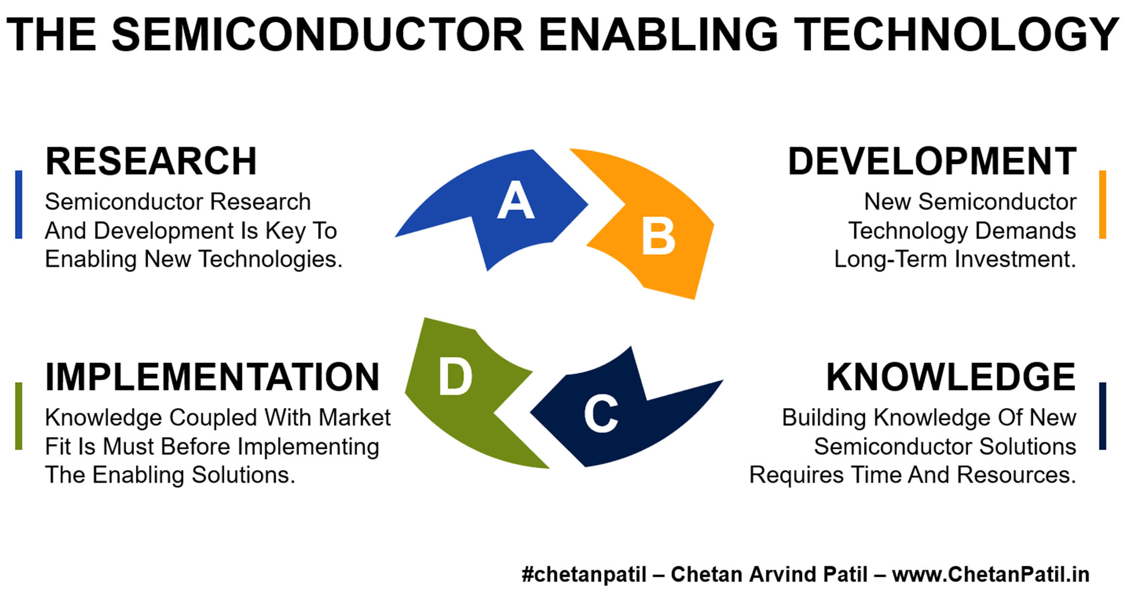
Research: Semiconductor Research And Development Is Key To Enabling New Technologies.
Development: New Semiconductor Technology Demands Long-Term Investment.
As with several high-tech industries, the cost to research and develop a semiconductor product is very high. Therefore, it makes the process of developing new solutions crucial and fragile. It also means investing in resources for the long term along with a backup plan in case of failure.
Knowledge building is key to finding if there is a fit for the new semiconductor-enabling technology. It focuses on ensuring the processes or new solutions developed will not only provide new features but will also fit in the semiconductor roadmap to bring the much-needed benefits.
Building knowledge is about capturing the correct information by empowering the right resources. And doing so requires experienced talents who can figure out the possibilities of new semiconductor enabling technology and how it will best fit the requirements of future products.
Knowledge: Building Knowledge Of New Semiconductor Solutions Requires Time And Resources.
Implementation: Knowledge Coupled With Market Fit Is Must Before Implementing The Enabling Solutions.
An example is an interposer. It not only found the perfect fit, but the solution pushed the semiconductor packaging industry towards a new era.
As the semiconductor industry moves forward, more semiconductor solutions will reach different types of technical and business walls, and to overcome them, more futuristic semiconductor-enabling technologies will play a key role, and now is the right time to develop such solutions.


