Photo by Nenad Grujic on Unsplash
Heterogeneous Integration (HI) has become one of the most focused topics in the last decade. From academia to industry, everyone is publishing and launching innovative solutions to scale transistors per area out of the die. HI is also one of the paths (that soon) all of the semiconductors companies will have to follow for high-impact and core systems like XPUs.
For every new technology, there are basic blocks that are required to ensure the new technology is adopted speedily. The list of blocks can be endless and varies from technology to technology. The same is valid for new semiconductor technology, and the challenges become tenfold due to the time, cost, and resources required to make an idea work error-free.
HI also requires several new and old building blocks to come together. Few of these blocks have been in use for decades (in the semiconductor industry), can be directly applied to HI. On another side, some blocks must get adopted for the HI.
A couple of examples of such blocks are interconnected and standards.
Interconnects: Interconnects are vital in driving the data transfer rate, and that too without adding any bottlenecks. For HI, electrical interconnects can introduce bottlenecks and thus demand new solutions. Optical and Optical-Electrical are two approaches that HI systems are increasingly adopting to solve bottlenecks. In HI, die-to-die interconnect also becomes crucial apart from silicon/die-only interconnect. A perfect combination of die-level and die-to-die interconnect is vital for HI solutions.
Standards: In HI, the die can come from a different vendor (due to IP) or the same vendor. However, to drive efficient integration, die-to-die level standardization is required. One such example of standards is Advanced Interface Bus (AIB). As more companies come up with HI solutions, it will be crucial for all to come together and move forward with HI-focused industry standards.
Apart from interconnects and standards, the other two critical building blocks vital for HI: testing and security. In the end, to make a HI solution defect-free, the building blocks required will evolve, but it is good to make a few blocks of HI robust. Importantly, to increase the adoption rate.
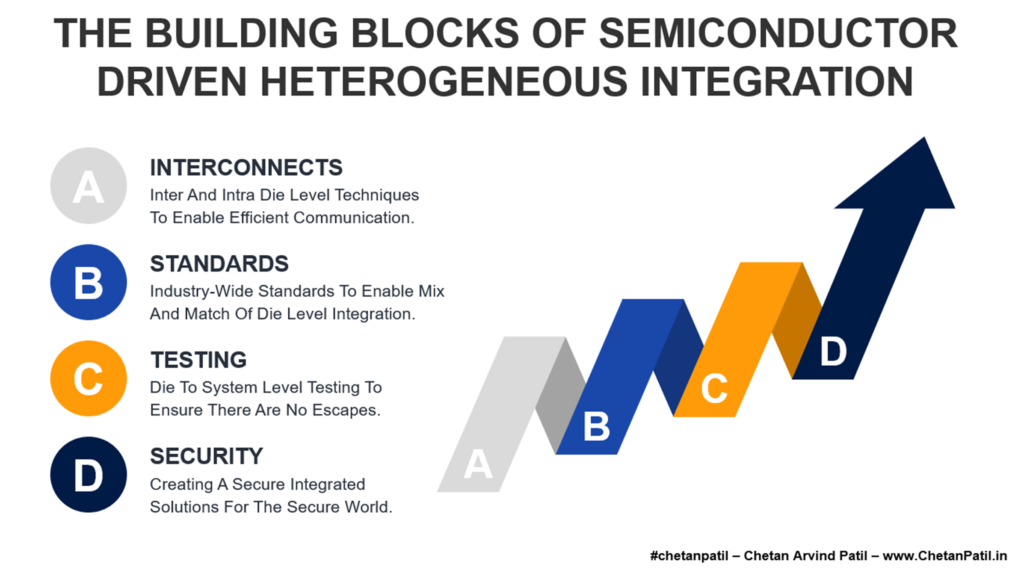
Testing and security are other major building blocks of the HI world. These two together ensure the end HI-inspired semiconductor product meets the strict requirement of the industry. Without proper testing, there can be escapes that can lead to failures in the field, and similarly, without security, the product can be compromised.
Testing: Testing ensures all the parts and sub-blocks within a die work as expected. For HI, this process changes a bit as the testing now needs to occur at a multi-die level. The testing world will still follow the individual die-to-die testing plan, but it is equally vital to ensure the multi-die (something like chiplets) work as it should. It certainly requires new methods, equipment, and skills.
Security: Like monolithic chips, HI-driven chip development also demands secure solutions. During HI, it becomes more about ensuring no counterfeiting, which may occur with multiple moving parts. Thus, it requires a secure supply chain for a secured HI world.
HI provides a long-term incentive for the semiconductor industry by ensuring the next-gen solutions will not be defined by the technology-node. Instead, chip development will get ranked based on how they leverage different die level techniques to bring an integrated way to design and fabricate future chips.
One of the challenges for the HI solutions is the cost and time to manufacture. Taking the die level solutions and manufacturing it into multiple dies and then integrating is costly and requires capacity, and both are very difficult to balance.
Irrespective of where the semiconductor industry heads, the chip development process will become more HI, and it will open up new opportunities for the semiconductor design and manufacturing world.


