
Photo by Jaromír Kavan on Unsplash
THE BUILDING BLOCKS OF SEMICONDUCTOR LOGIC TECHNOLOGY MAP
The transistor is one of the building blocks of the semiconductor industry. It has also gone through drastic transformation led by very high activity of research and development. These transformational changes, year on year, have empowered the semiconductor industry in providing solutions that are 2x faster and occupy 2x less space.
Optimization activities have not stopped, and now companies and academia are gearing up to target next-gen solutions that will drive the semiconductor solutions into the More-Than-Moore era. And, to drive next-gen transistors, different research entities (semiconductor FABs and FAB-LESS) must focus on a semiconductor logic technology map.
FAB/OSAT Map: Provides an overview of how semiconductor technology will progress within a given FAB and OSAT.
Logic Technology Map: Provides an overview of how the device/transistor level technology will progress to enable next-gen logic devices.
The sole goal of the semiconductor logic technology map is to come up with new ways to enhance transistors. Developments around semiconductor logic technology map are the reasons why today the semiconductor industry has seen different types of transistors: PlanarFET, FinFET, GAAFET, and now MBCFET.
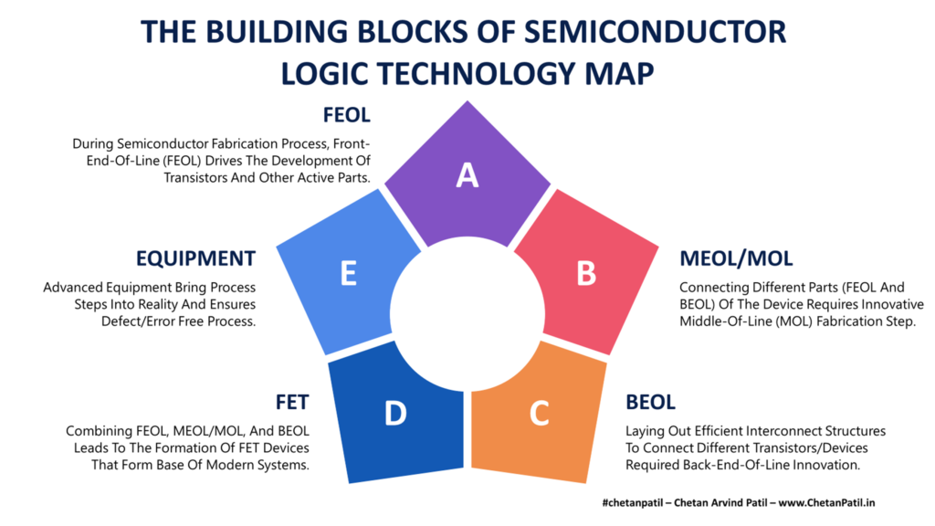
FEOL: Front-End-Of-Line is the backbone of semiconductor devices. The way FEOL technology progresses drives the technical characteristics of the devices/transistors. Time to turn on/off without adding delay is also one of the focuses of FEOL devices. FABs are dependent on FEOL and often have to work relentlessly in ensuring the new process is improved correctly to bring new technology-node.
MEOL/MOL: Middle-End-Of-Line/Middle-Of-Line builds the connection between FEOL and BEOL, and acts as a catalyst by providing tiny structures that allow the pathway between the front and back end of the semiconductor device development. As the complexity of the transistors has increased, so has the process to create tiny structures between the front and the back end side. The complexity and the importance make MEOL/MOL a critical logic block.
BEOL: Back-End-Of-Line takes the help of different types of metal structures to provide an interconnect between different types of transistor devices. BEOL ensures that devices interact, and the chip is active and always working as per the design.
FET: Transistors development is tied to how FEOL, MEOL/MOL, and BEOL evolve. In the end, customers are focused on how the power, performance, and thermal profiles of next-gen FET transistors. Such key metrics can make or break the next-gen FET adoption. Given the dependence on FETs to enable the vision of building efficient products, FETs are one of the crucial blocks of the semiconductor logic technology map.
Equipment: It is not possible to drive the development of new semiconductor processes without advanced equipment. Semiconductor equipment manufacturers have to work closely with the FABs and research team focused on bringing next-gen FET. It ensures that the new equipment is capable of driving the vision into reality. In many cases, the pros and cons around the equipment technology (EUV) can decide the fate of whether the research/theory can be brought into reality or not.
Building blocks of semiconductor logic technology map ensures that the next-gen devices keep getting launched. Thus can also provide process-level solutions to the customers to make the most of their designs.
It is crucial for Pure-Play or IDM to come up with a clear long-term semiconductor logic technology map that can excite their customers and allow them to make most of their design from a power, performance, thermal, and operating voltage point of view.
THE KEY TO BUILDING SEMICONDUCTOR LOGIC TECHNOLOGY MAP
The building blocks of the semiconductor logic technology map are well known to the majority of the industry. What sets a specific semiconductor entity apart is the resources required to drive the semiconductor logic technology map.
Research and development to enable next-gen logic solutions/transistors require long-term planning. It is also one of the most highly resource-demanding processes and takes years (even decades) to validate the theory.
To increase the success rate of such a long-term process, different semiconductor logic-focused stakeholders (academia and industry) need to drive key activities to build a robust semiconductor logic technology.
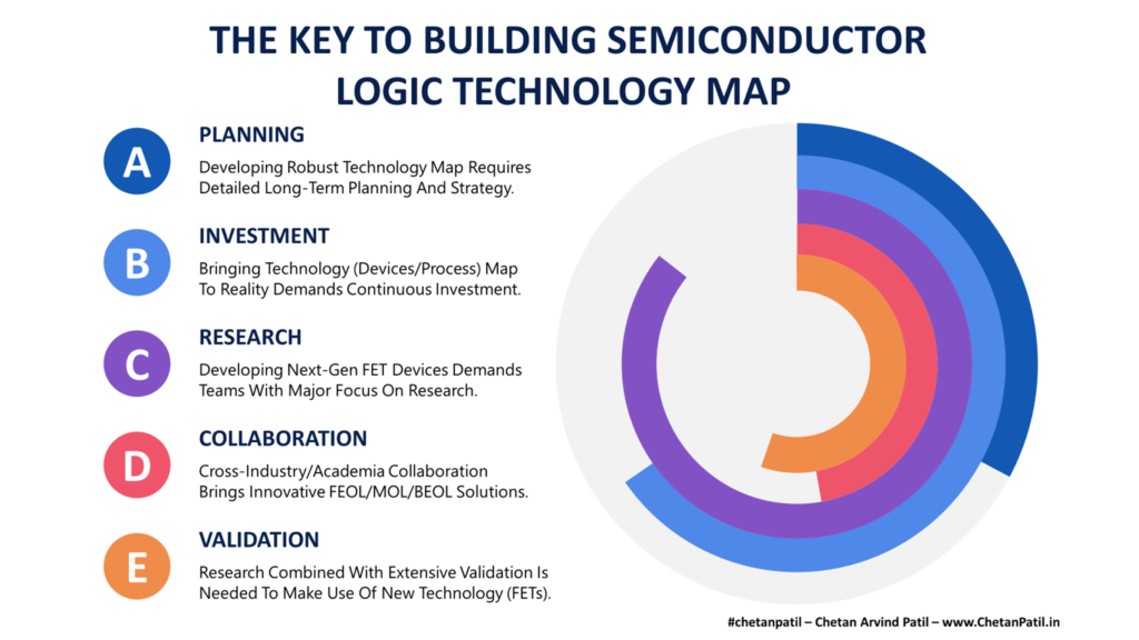
Planning: A long-term planning enables teams to focus on solutions that can bring efficient logic devices into the market. There are so many areas within the semiconductor fabrication process. Hence, it becomes critical to have a dedicated yearly (or five-year) plan to bring new devices into the market to ensure the customers understand how new solutions will drive future semiconductor products.
Investment: Planning requires investment, and it is critical to invest in specific resources that maximize outcomes. Whether forming technical teams or building new advanced labs with modern equipment, all require long-term continuous investment. Thus, investment (and that too continuous) towards the next-gen device is critical.
Research: Planning combined with investment can drive very high research activity. Research requires a dedicated academic team or a mix of industry and academia. In the end, the goal is to come up with logic-level solutions to ensure the next-gen device is more advanced than any of its predecessors. Hiring the right resources for logic research activities is crucial too.
Collaboration: Proper planning, investment, and research often require a collaborative approach. It can be cross-industry or cross-academia. Whichever path, the end goal is always to ensure the collaboration often leads to fruitful results. Collaboration is often a differentiating factor of all the highly advanced solutions in use today compared to those which didn’t end up getting used.
Validation: Planning combined with investment and research-driven by active collaboration is fruitful only if the theory is validated. The validation demands a dedicated facility (FABs, Labs, Equipment, etc.) that can drive the validation process to ensure the new logic solutions aligns with the theory. Lack of validation can break the years of research, and the validation process also enables customers to capture the pros/cons of new logic solutions.
Years and decades of shrinking transistor size have allowed the industry to provide new semiconductor products. To continue the momentum (beyond the angstrom era) of semiconductor logic technology map means bringing different key blocks to work together in harmony.
It takes years of effort to bring next-gen semiconductor logic solutions into the market. Then another few years to break even around the new proposed solutions. To ensure all such goals get achieved in a time-bound manner, semiconductor companies need to plan and openly share the logic technology map.


