THE COMPLEXITY OF SINGLE-TECHNOLOGY-NODE ARCHITECTURE
To ensure high-speed processing, one active component in a computer system – the Central Processing Unit (CPU) – has seen numerous technological advancements.
The CPU advancements have been distributed equally on the design and the manufacturing aspect of the semiconductor development process, both driven by Moore’s law.
Design: During the pre-internet era, the CPU used to get designed to handle basic input/output tasks. For such requirements, the data and memory handling were not complicated as it is today, and a single-core/unit of CPU could do the required task. As the world moved towards the digitization brought forward by the post-internet era, the multi-processing solution came to use. The next decade or two saw innovative CPU designs alongside the active components like GPU, Memory, Interconnect, ASIC, and FPGA.
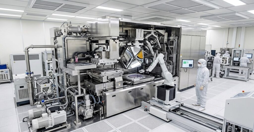
Manufacturing: In 1990, the Intel P5 Pentium used an 800 nm technology-node, and in 2021, Intel is planning to move towards a third-generation of 10 nm with its Alder Lake series of microprocessors. Intel’s competitor AMD has already taken the lead with its 7 nm technology-node. Mobile and smart domains are already using a 5 nm technology-node and marching towards 3 nm.
The exploding data-intensive, compute-intensive and memory-intensive computation is now pushing the world from the general-purpose to specific-purpose computer architectures.
However, the foundation for a specific-purpose architecture was laid long back by System-On-A-Chip (SoC). SoC is an integrated chip that incorporates not only CPU but also other active components like the GPU, Wireless Chips (Cellular/Wi-Fi/Bluetooth/GPS/NFC), Memory, ASIC (Different types of XPU), and in some cases combined with FPGA to form SoC-FPGA.
SoC is vital for mobile devices and solutions where there is not much room to take advantage of the form factor. For a data center, there is the possibility to split out the GPU (and other XPU) as a co-processor (huge is size) with its power and cooling techniques. However, the same is not feasible for a mobile device like a smartphone or any IoT device.
Semiconductor Manufacturing Will Hit Technology-Node-Wall, Driving The Need For Multi-Technology-Node Architecture
On top of this, every block inside the SoC is fabricated using the same technology-node. This brings design and manufacturing complexity as the transistor size keeps shrinking. The design to fabrication to testing to packaging challenges added due to new technology-nodes eventually adds costs, apart from the cycle time required to prove the working of the new products with new generation of the technology-node.
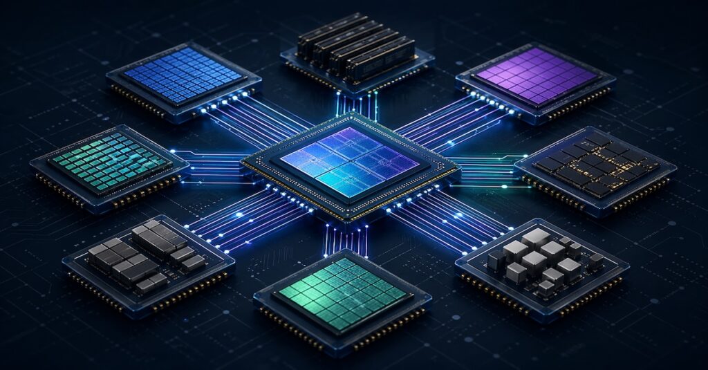
To overcome cost and other technical challenges brought forward due to advanced technology-node, a new approach to design and fabricate the SoC’s internal blocks using different (new/lower and old/higher) technology-node needs to be explored. This design approach can be termed as Multi-Technology-Node Architecture.
What Is Multi-Technology-Node Architecture:
Design And Fabrication: Ability to design and fabricate active blocks inside the SoC with different technology-node. GPU can be at 14 nm while CPU is at 7 nm.
Technology-Node: The transistor size within each block follows a specific technology-node. Different blocks can use different technology-node.
Interface And interconnect: Packaging the blocks with different technology-node separately and sticking together with the help of a high-speed interface and interconnect.
Memory: Unified high-speed and high-bandwidth memory with its own technology-node to enable faster data flow.
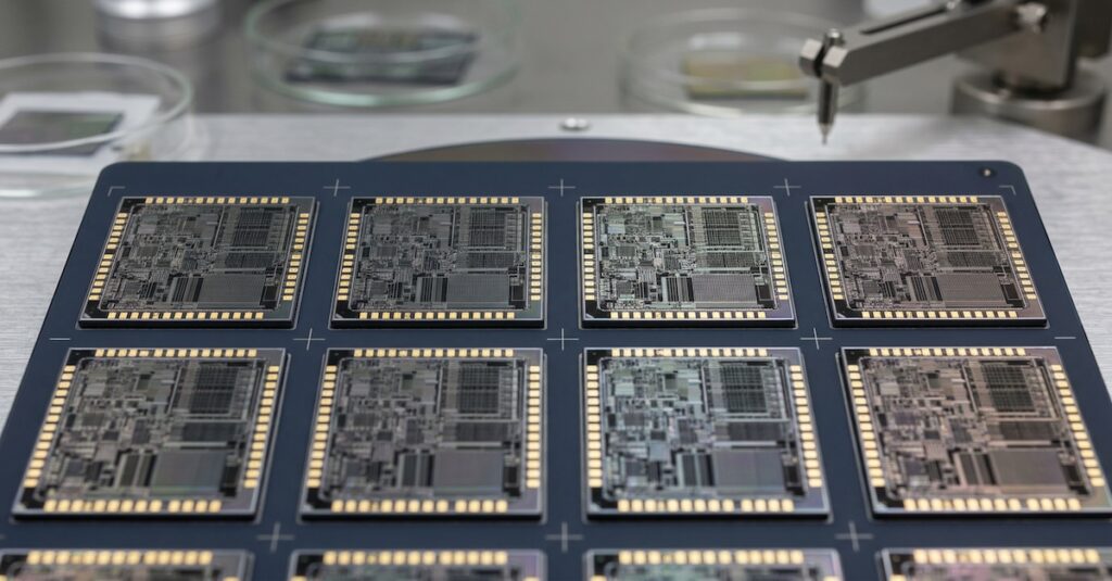
Testing: Each block of SoC fabricated with a different technology-node can be tested separately before packaging.
Packaging: Follows System-In-Package (SiP) and other related heterogeneous packaging processes to stitch the all blocks of SoC fabricated using different technology-node.
The major advantage of Multi-Technology-Node Architecture will be the ability to balance the cost and cycle time.
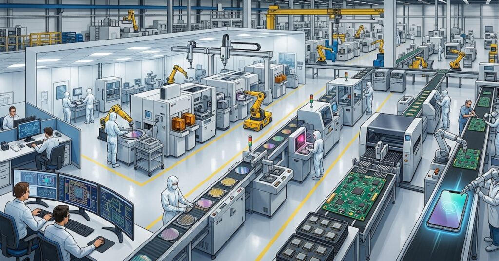
The cost of fabricating some components as a separate die with high technology-node (more than 14 nm) and then packaging it to alongside blocks using advanced technology-node (7 nm or less) has the potential to lower the cost of fabrication and manufacturing. It also means the blocks of SoC can be fabricated at a different location and then packaged at the OSAT for validation, thus lowering the cycle time to market due to parallel fabrication.
Multi-Technology-Node Architecture will also drive IP based SoC block-level solutions that can bring more innovation in the SoC semiconductor space.

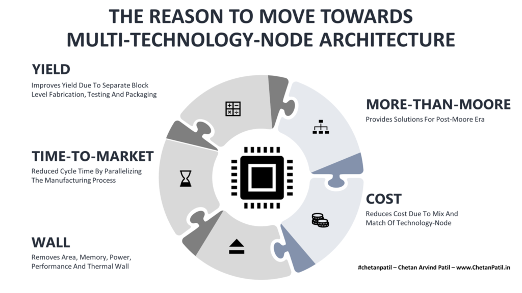
THE REASON TO MOVE TOWARDS MULTI-TECHOLOGY-NODE ARCHITECTURE
There are numerous reasons (and benefits) as to why computer architecture design and manufacturing should move towards multi-technology-node architecture:
Yield: Putting so many blocks together inside an SoC using a single-technology-node architecture design (Example: 7 nm technology-node) brings complexity. It puts constraints not only on the fabrication side but also on testing and packaging. The high-yield for every wafer fabricated with the SoC becomes a difficult task. The electrical testing itself needs to be detailed to ensure that the blocks are working as per the specifications. This complexity quadruples at advanced technology-node like 5 nm and lower. Using multi-technology-node architecture ensures that the different blocks are designed and fabricated with different technology-node. All the higher technology-node (more than 14 nm) are already proven in the market, and this speeds up the fabricating to testing processes. It also massively helps eliminate waste and improves the yield.
Time-To-Market: Proving out the solution at a specific advanced technology-node (using single-technology-node architecture) takes time with numerous SOC components that need to be carefully designed and fabricated in a single die. Any issue with the design or manufacturing eventually increases the time taken to launch the product in the market. Given how stiff the competition is in the semiconductor industry, any delay can cause loss and market position. With multi-technology-node architecture, only specific blocks using new technology-node needs to be more focused on to ensure correctness. The rest of the blocks can take advantage of higher technology-node that have been in use in the market for years and have proven semiconductor process/product.
Wall: The SoC is designed mainly for mobility. Even today, there is no way to provide unlimited direct power to the devices using the SoC in a mobile scenario. Eventually, one has to rely on battery technology to bring mobility. However, fabricating components with thousands of transistors consume power, and improving performance-per-watt (PPW) is becoming a challenge. The SoC design will soon run into area, memory, power, performance, and thermal wall with single-technology-node architecture. Multi-technology-node architecture can provide avenues to bring new ways to manage thermal constraints (using innovative IP from different semiconductor companies) apart from lowering power consumption due to the no area constraints/requirements and also the usage of different types of technology-nodes.
Cost: Shrinking transistor size means adding more manufacturing capacity. The Pure-Play Foundry and IDM have to keep investing in new equipment and process recipes to ensure that the next technology-node is available within two years for any new technology-node launch. All this puts a lot of CapEx pressure on the manufacturing aspect of the SoC using single-technology-node architecture. Apart from manufacturing, the design houses (FAB-LESS/IDM) also have to keep investing in new R&D activities to bring innovation in transistor/device design to enable advanced technology-node process development. With multi-technology-node architecture, existing manufacturing capacity can be used efficiently.
More-Than-Moore: The semiconductor industry is trying to grappling for More-Than-Moore solutions. While there have been many designs for manufacturing processes that are catering to more-than-Moore solutions, multi-technology-node architecture is another approach that takes away the pressure of using the same-technology-node for every block of the SoC. Thus, giving way for another More-Than-Moore solution.
Apart from the above benefits, multi-technology-node architecture brings challenges too. It will require end-to-end semiconductor process validation before being used on a large scale.
THE BOTTLENECKS FOR MULTI-TECHOLOGY-NODE ARCHITECTURE
Multi-Technology-Node Architecture is not in use today. Few years down, it might be a possibility, and to ensure such architecture technique can be fabricated with the blocks of SoC using different technology-node, the following are the two bottlenecks:
Research And Development: Understanding the technical constraints of fabricating blocks of SoC using different technology-node requires research and development efforts. This is to ensure that there is no escape in the architectural process that leads to bigger issues than relying on a single-technology-node architecture way of designing SoC. A close three-way collaboration between Academia, FAB-LESS/IDM, and Pure-Play/IDM is required. Such collaboration requires time to show results. Hence, the research and development activities for multi-technology-node architecture should start today, not tomorrow.
Investment: Initial investment required to prove out the multi-technology-node architecture solutions is high. It requires investing in new software and hardware tools, in order to ensure that the SoC blocks fabricated separately can work in harmony and there are no technical constraints about which technology-node a given blocks used. The semiconductor packaging solution to allow multi-technology-node architecture integration will also be costly due to low scale usage.
As the semiconductor design and manufacturing companies start looking into the possibility of a multi-technology-node architecture, there might be more technical to non-technical bottlenecks apart from the above two.
In any case, multi-technology-node architecture has the potential to provide Post-SoC era computer architectures.


