Semiconductor products often fail, and finding the root cause thus becomes a critical process. More so, when the product is already in production.
Failure and root cause analysis are vital steps towards finding issues with the semiconductor product. Doing so requires an inspection process that allows engineers to look inside the chip.
Several advanced equipment and technologies (SEM and beyond) can provide an in-depth view of what is happening inside the chip. The hurdles thus are not the availability of technology required to drive failure analysis. The real challenge is the complexity (silicon level) that the advanced design and manufacturing brings to enable failure analysis.
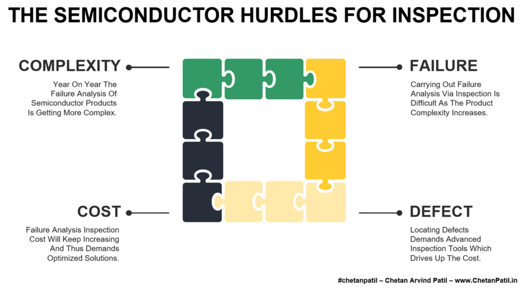
Complexity: Growing transistor count increases the die level complexity, which brings difficulties to perform failure analysis without investing more than the required time, resources, and capital.
Failure: During failure analysis (in the majority of the cases), it becomes difficult to narrow down the root cause for highly complex (3nm and lower) products. Advanced equipment does help, but not without investing a lot of time and cost.
Overcoming different inspection hurdles is a vital step towards a fast resolution of why the product failed. At the same time, the growing design complexity of semiconductor products (coupled with different package technologies) is leading to constant upgrades of labs that enable such analysis and leading to the high cost of finding the defects in the product.
The fundamental process when carrying out failure analysis is the localization of defects. Doing so requires semiconductor products to run through several inspection steps, and it often requires looking at every layer. Biasing process helps, but it requires skilled engineers with years of experience to handle the inspection tools to find areas of concern within a given chip.
Defect: Year on year, the localization of defects during the failure analysis is getting costlier and time-consuming. All of this leads to constant upgrades of equipment apart from the training of engineers.
Cost: The cost of inspection to capture the failures is increasing due to the need to constantly upgrade labs apart from the time required to find defects in the highly complex products with advanced technology nodes. Solutions like do SEM are helpful but are also high on cost.
Today’s advanced semiconductor product utilizing the latest technology node often comes equipped with billions of devices. Inspecting such devices is certainly not an easy task. More so, when the goal is to quickly root cause silicon-level issues.
The importance of inspection as part of a semiconductor product (in case of failures) will only grow with the growing number of transistor counts. It is thus vital to focus on optimizing the process to perform failure analysis so that the operating cost is reasonable while also bringing skilled engineers who can efficiently carry out inspection-driven failure analysis.


