Photo by Vishnu Mohanan on Unsplash
THE GROWTH OF DATA IN THE SEMICONDUCTOR MANUFACTURING
The growth of digitization has led to the generation of massive amounts of data on day to day basis. The data explosion has pushed several industries to adapt to data-driven analysis and decision-making processes. The same is true for the semiconductor industry.
Data was always an integral part of semiconductor design and manufacturing. The need for data has increased further due to the cost and risk involved in designing products that are becoming smaller and smarter. The cost to fabricate semiconductor products is high and that is why during the design phases innovative simulations/modeling approaches are used to validate product design against specification before sending the final design files to the semiconductor fabrication houses. The risk of not spending time to collect and review semiconductor data both during the design and the manufacturing stage can cost a lot of money and time if the product starts failing in the field.
Data-Driven Approach Is Raising The Bar Of Semiconductor Manufacturing
As the technology-node and package technology have advanced, so needs to take a data-driven approach to semiconductor manufacturing. The goal of the data-driven approach is to ensure that the products being are defect-free. The sophisticated tools and equipment used by the semiconductor manufacturing process have only gotten more advanced. The de-facto feature of these system-driven tools is to capture data and present it in a form that makes the decision-making process easier and faster.
The data-driven approach is required to meet the following two important requirements of semiconductor manufacturing:
Quality: Qualifying every semiconductor products is vital. It has to meet different industrial standards. Automotive semiconductor products have to go through one of the most stringent qualifying processes to ensure the product can work seamlessly everywhere. It is vital to ensure the manufacturing process established meets the high standards of quality requirement, which is possible only if the data captured to drive the decision-making process.
Waste: Every data point tells a story. In semiconductor manufacturing, data can be about the design or the manufacturing tools, or handling issues, and many more. Every semiconductor data type counts towards ensuring the wafers and assembled parts are not getting scrapped. Scrapping raises yield concerns and indirectly impacts the cost.
Without investing time and money in the data-driven approach to manufacturing semiconductor products, the semiconductor companies run into the risk of overlooking the quality metric. Driven by the need to ensure the products using the semiconductor solutions meet user satisfaction, the customers/companies using the semiconductor products are increasingly using Defective Parts Per Billion (DPPB) as a new metric than Defective Parts Per Million (DPPM).
The need to capture, process and review semiconductor manufacturing data is becoming vital when there is a possibility that the semiconductor device might end up powering critical infrastructures likes satellites to aerospace to automotive (and many other solutions).
All this is why the semiconductor industry is becoming more data-driven than ever before. The manufacturing part of the semiconductor process is not complete without letting the data speak.
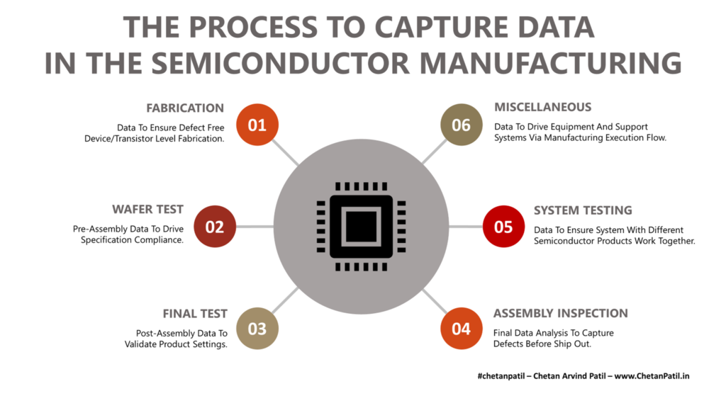
THE PROCESS TO CAPTURE DATA IN THE SEMICONDUCTOR MANUFACTURING
The semiconductor manufacturing process is a well-established flow. While every product has different requirements driven by the specification it is supposed to work within, some standard flows/stages are common across numerous semiconductor products.
These processes use tools/solutions/recipes to capture data, which eventually drives a data-driven decision-making approach in semiconductor manufacturing.
Following are the major process that leads to capturing of semiconductor manufacturing data:
Fabrication: The first step towards semiconductor manufacturing is to fabricate the product on the wafer. Every layer/mask/stage of the semiconductor device fabrication is data-driven. If the data does not align at the etch or the lithography stage (for example), the wafer/lot cannot move forward. Several modules are placed in the kerf region of the wafer to data of the devices (that eventually make up the full die) to ensure is no deviation in the semiconductor wafer. All this data is unique to the technology-node. At the end of the wafer fabrication, data in the form of visual images ensure no particles or scratches are present on the wafer/die.
Wafer Test: The defect-free wafer coming from the semiconductor fabrication facility gets sent to the test facility. The wafer test stage ensures all the die on the wafer gets electrically tested with the test program to validate whether the die meets the specification or not. The good and the bad die are marked accordingly. All this is possible due to ATE tools and probing hardware. The data is analyzed to understand any excursion, which eventually gets debugged to ensure no test escapes.
Final Test: The final test can be performed on the wafer (Wafer-Level Chip Scale Package (WLCSP)) or on the assembled parts (non-WLCSP). The final test uses similar testing criteria and tools like the wafer test). The major difference is the packaging testing versus dies testing. The data points are specific to the package testing. This is often the last electrical data point the semiconductor manufacturing process generates before the parts are shipped to the end customer or assembly.
Assembly Inspection: Post assembly, the visual inspection of the assembled parts is carried out. The tools used for visual inspection capture all sides of the assembled parts. The data in the form of images show if chipping/defects occurred during the assembly process. If so, then the root cause needs to be determined. The data in the form of images often requires a highly automated system to alert any defects.
System Testing: A final system (like a smartphone) not only uses one specific semiconductor product but several others. All the different semiconductor products are assembled onto the Printed Circuit Board (PCB) and should work in harmony. If anything fails, then the data relevant to the failing semiconductor product is capture and sent to the company that fabricated it. System testing also drives the semiconductor manufacturing process from the customer side.
Miscellaneous: The last data point in the semiconductor manufacturing are from the equipment that enables the different process. These need periodic maintenance to avoid breakdown. All the equipment connected via a Manufacturing Execution System (MES) is monitored to capture every activity the equipment/tools perform. This data is vital for keeping the semiconductor manufacturing facility up 24x7x365.
The above data points are vital in ensuring the semiconductor manufacturing process is fabricating/testing the high-quality products that meet the stringent quality requirements. To ensure, the high-quality demand data-driven process is critical in semiconductor manufacturing.
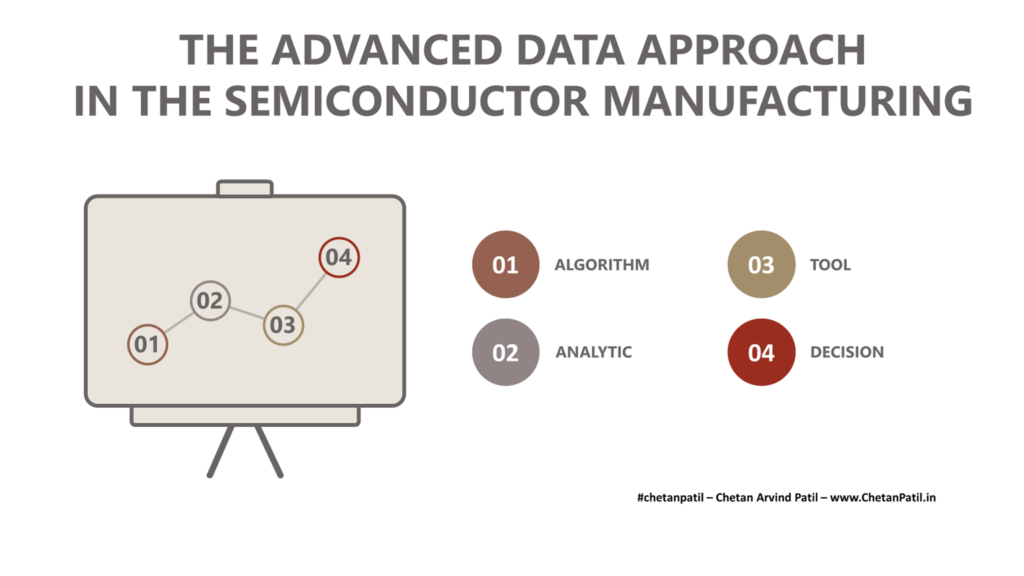
THE ADVANCED DATA APPROACH IN THE SEMICONDUCTOR MANUFACTURING
Even though data exploration in semiconductor manufacturing is not new, the need to take a different data analysis approach is growing. The main reason is due to the high cost required to generate the semiconductor data. In the smallest data available, the semiconductor engineers need to predict that the products will work in the market as per the specification.
To lower the time taken to move the wafers to the next stage, the semiconductor manufacturing process is relying on different advanced approaches to enable data-driven semiconductor manufacturing:
Algorithm: Due to the proliferation of fast systems that can crunch data on the go has led to the development of algorithmic solutions that can detect scratches, clusters, excursions, particles, etc., faster than ever. The algorithms deployed can capture the patterns to raise an alert if there are issues with the semiconductor manufacturing process. These algorithms take the help of numerical data or visual data. Visual data is more vital as it shows gate-level details using an advanced microscope. There are already solutions, but there is a need to minimize the time taken for decision making as spending more time to decide on the correctness of the product means holding the lot/wafer from releasing, which can be costly.
Analytic: Data lying without insights is not useful. Given that every die/chip that gets shipped out of the semiconductor manufacturing flow is visualize/tested, it is important to develop an analytical approach that uses computational analysis of statistics to drive data exploration. It helps the semiconductor data engineers to visualize data using diverse statistical methods to find issues/outliers. Analytical solutions are already available in the market/industry, but often requires skills to look beyond what is being presented on the dashboard.
Tool: Tools are required to view the detailed history of every die that gets manufactured. The standard process to capture and store is already defined. The end-to-end semiconductor manufacturing data analysis still requires different tools to visualize and critically analyze the data. One single data tool may not be enough. It is good to test and use data analytical tools (or programming methodologies) as per the need to drive the decision-making process.
Decision: Eventually, the goal of data analysis in semiconductor manufacturing is to either hold or release the product. It requires the perfect combination of computer and human. Computers can enable data collection and storage. However, the data wrangling is still on humans. In semiconductor manufacturing, every new data requires a new inspection approach as every new product is different from the last one. All this means every changing data-driven approach to decision-making (hold or release).
The speed at which the semiconductor industry is driving towards the shirking technology-node year-on-year, the process to scrutinize the data will also change, and the semiconductor data inspection process will keep getting directed towards new ways to enable the smarter data-driven approach towards the semiconductor manufacturing.


