#chetanpatil – Chetan Arvind Patil

Semiconductor Fabrication

Photo by Mathew Schwartz on Unsplash.

Samsung’s technical blog has series of articles on semiconductor fabrication. It covers majors steps from tape out to packaging. All nine parts of the series are not linked together, so I thought of creating a list that may help those interested in learning about semiconductor manufacturing.

All the images below are from respective part of the series linked in the title.

Part 1: Creating the Wafer

Picture By Samsung

Part 2: The Oxidation Process

Picture By Samsung

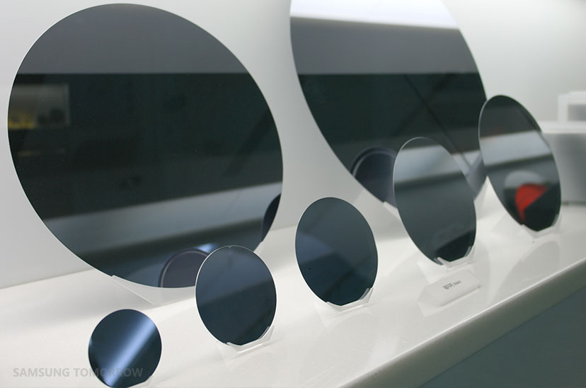
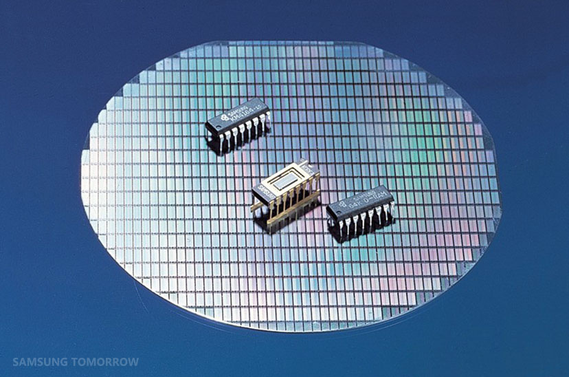
Part 3: The Integrated Circuit

Picture By Samsung

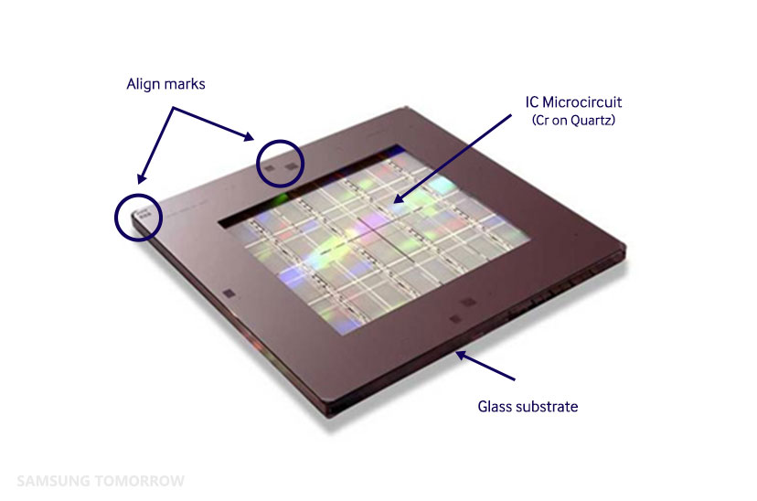
Part 4: Drawing Structures in Nano-Scale

Picture By Samsung

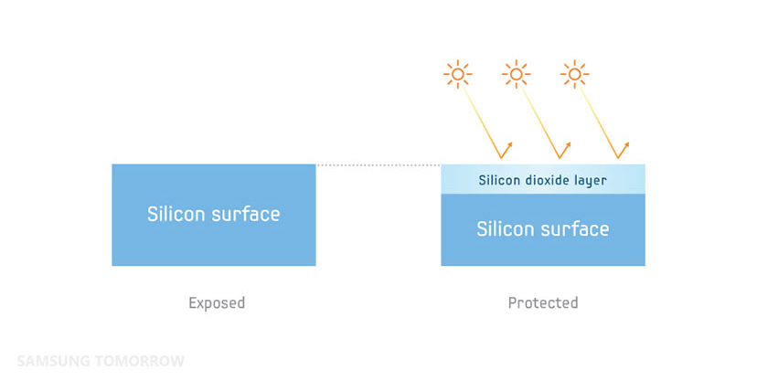
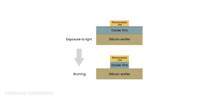
Part 5: Etching A Circuit Pattern

Picture By Samsung

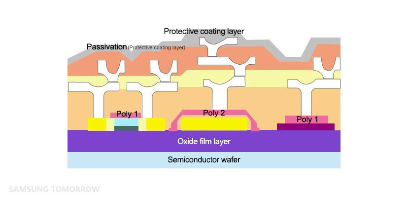
Part 6: The Addition of Electrical Properties

Picture By Samsung

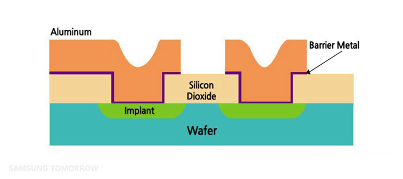
Part 7: The Metal Interconnect

Picture By Samsung

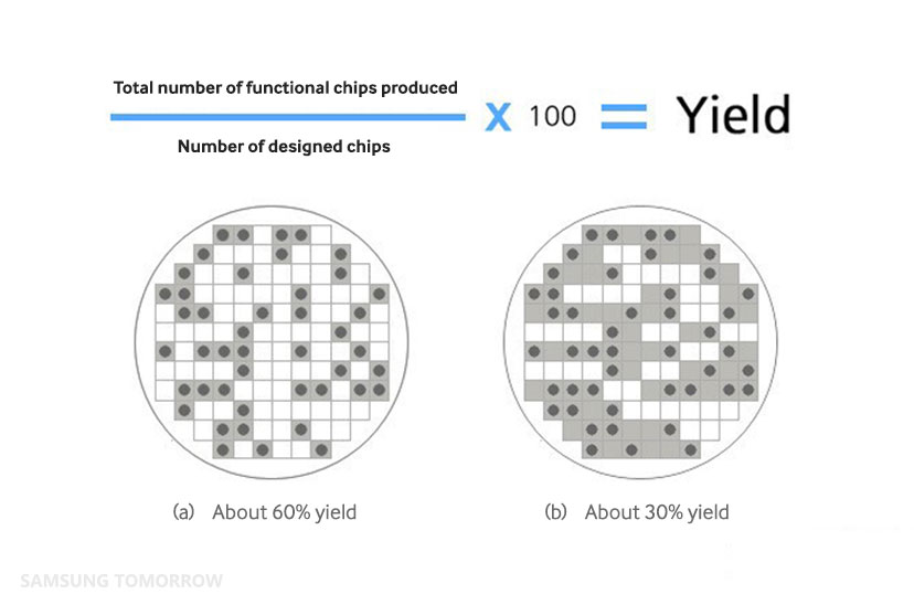
Part 8: Electrical Die Sorting (EDS)

Picture By Samsung

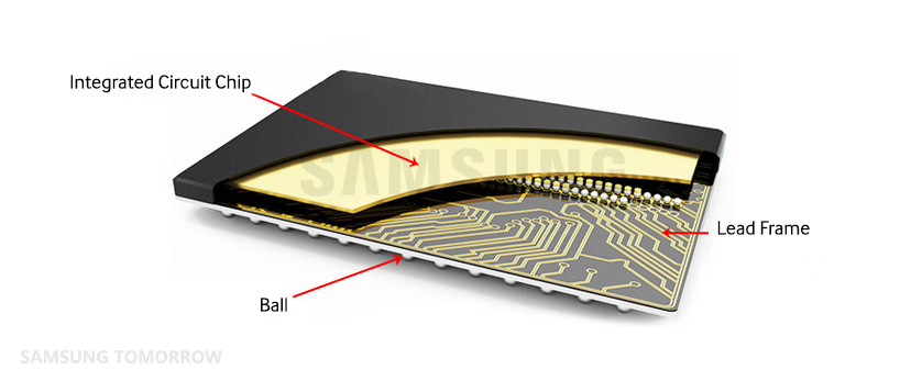
Part 9: Packaging and Package Testing

Picture By Samsung
Chetan Arvind Patil

Chetan Arvind Patil

                Hi, I am Chetan Arvind Patil (chay-tun – how to pronounce), a semiconductor professional whose job is turning data into products for the semiconductor industry that powers billions of devices around the world. And while I like what I do, I also enjoy biking, working on few ideas, apart from writing, and talking about interesting developments in hardware, software, semiconductor and technology.

COPYRIGHT 2024, CHETAN ARVIND PATIL

This work is licensed under a Creative Commons Attribution-NonCommercial-ShareAlike 4.0 International License. In other words, share generously but provide attribution.

DISCLAIMER

Opinions expressed here are my own and may not reflect those of others. Unless I am quoting someone, they are just my own views.

MOST POPULAR

RECENT POSTS

Get In

Touch