
Photo by Laura Ockel on Unsplash
THE SEMICONDUCTOR AS A SERVICE
The software industry has adapted to the demand of business and consumers by changing the licensing and product delivery model over the last three decades. The post-1990 saw standalone one-time fee-based software with no incremental feature updates except security-related and termed as the pay and use model. Then post-2000, with the proliferation of the internet, the software license model moved to pay over month/year and also came with features and security updates. The software industry termed it as Software-As-A-Service Model. Post-2010, the software industry adapted to the changing business and applied the licensing model from software to platform, which came not only with features and security updates for the software itself but also the platform the software will run on. It has allowed software developers to provide more over the top services.
In comparison to the software industry, the hardware industry (mainly the semiconductor industry) has not adopted the product delivery model. It has been constant and driven by build and ship, with no ability to provide new hardware features on the go. If there are security flaws in the hardware, then those are suppressed by an Over-The-Air (OTA) update. Consumer and business buying the piece of silicon get locked in with the product. It is also not easy to provide new features at the silicon level. On top, the majority of the products shipped by the semiconductor industry end up getting used differently based on the hardware company’s need.
The semiconductor products (from CPUs to NPUs to GPUs to ASICs to FPGAs to DSPs to Mixed/Analog/Digital devices) have a long design and manufacturing cycle. It also means a long-term vision of the future market needs and then aligning the investment in the design to the manufacturing process accordingly. As per the market demand, semiconductor products need to be more adaptable with in-built features that are more relevant a few years down the line and can be activated post-production.
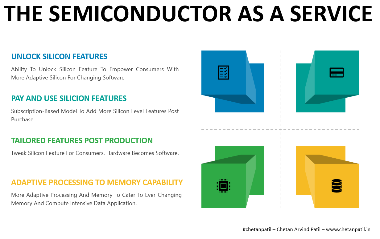
Semiconductor-As-A-Service Is Possible Today Than Ever Due To The Shrinking Transistor Size That Allows More Silicon Features To Be Built-In Today For The Future Needs.
The approximate life of a smartphone is anywhere between three to five years. However, the majority of companies stop providing critical software updates that make the smartphones redundant. The launch of new smartphones with new silicon and software grabs consumer’s attention and they end up buying a new smartphone with the latest silicon features.
Imagine, having adaptable silicon with features built-in that can be unlocked a few years later and thus making the hardware as new as the software? Either vendors or consumers can decide which silicon features should be activated and how it helps the device performance. Such a process will allow the semiconductor industry to deliver silicon services under Semiconductor-As-A-Service model.
Semiconductor-As-A-Service – A product delivery business model for the semiconductor industry which allows silicon design and manufacturing with in-built silicon features that can be unlocked in the future as the market demand and software requirements align. For example – More graphics for new gaming applications. These silicon features can be enabled with the help of software updates and require a subscription or one-time payment license. The list of features can be endless, from more cache memory to DRAM memory to extra processing cores to additional GPU for gaming applications to secondary cellular (perhaps 6G) antenna. The shrinking transistor size and growth of heterogeneous integration as a More-Than-Moore (MTM) solution makes such features in silicon possible. Silicon area with extra features can reside inside the smartphone launched in 2020 as an inbuilt hidden feature with the option to enable in 2022 as long as consumers are willing to pay. Such service can also be bundled with software features wherein the smartphone manufacturers can tie the new feature like extra memory or storage.
THE PROCESS OF SEMICONDUCTOR AS A SERVICE
Semiconductor-As-A-Service implementation can unlock a plethora of opportunities not only for the semiconductor industry but also for the software industry. However, implementing Semiconductor-As-A-Service requires a specific process to be followed from designing to manufacturing. It also requires the semiconductor industry to take risks by providing advanced technology node use today rather than a few years down. Using advanced technology is the key to fitting more silicon features that can be unlocked post-production as it allows more silicon in the smallest possible area as this helps in providing more features at the transistor level.
Semiconductor-As-A-Service Process:
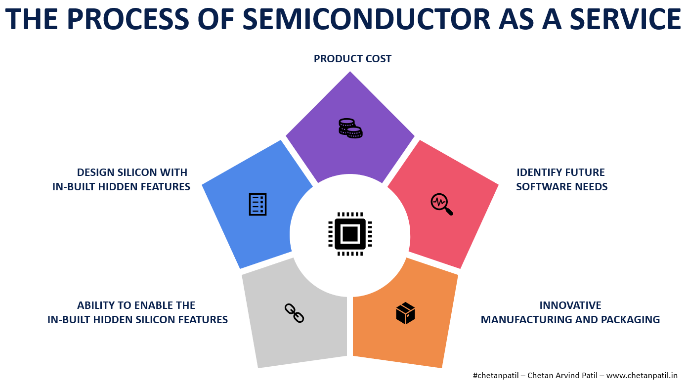
Identify Future Software Needs – These software features should be those that become bottlenecks for consumers. It can be from understanding whether the consumers will need more memory than the product has been shipped with so that with the growing data-driven application enabling an extra memory at the silicon level can cater to the software demand. The same goes for CPUs and GPUs for processing power.
Design Silicon With In-Built Hidden Features – Post identification of future software needs, packing the silicon with features that get unlocked in the future. The majority of these features will reside inside the System-On-A-Chip (SoC), as the active components are the ones that can provide more benefits of service-based features than passive components. Usage of advanced technology node is key to enabling such silicon level features.
Ability To Enable The In-Built Hidden Silicon Features – Incorporating the in-built hidden silicon feature requires not only designing it with secure memory to store keys to activate features but also requires a secure manufacturing process. The secure way of design and manufacturing ensures that there are no security flaws that can be exploited by hackers.
Innovative Manufacturing And Packaging – The critical piece of the Semiconductor-As-A-Service process is to ensure that the manufacturing flow and the packaging technology use advanced techniques to consider the effects when more silicon area is activated. Activating new features (more memory or processing capability) can have significant power and thermal effect.
Product Cost: Planting more silicon with the expectation that it will get used in the future under a pay-as-use service is a business risk. It is vital to price such products so that the design and manufacturing costs invested gets recovered even when in-built hidden features do not get utilized.
Above are the five key process steps that lay the foundation of Semiconductor-As-A-Service. It has the potential to make the silicon more adaptive. It will require massive research and development before the industry can use it as a real-world solution.
THE NEAR-TERM IMPACT OF SEMICONDUCTOR AS A SERVICE
If Semiconductor-As-A-Service is implemented and widely used, then it has the potential to transform the computing industry.
The ability to enable an extra layer of processing power on the go provides a new way to process data. With 3.5 billion 5G subscribers by 2026, the data consumption will skyrocket, and having silicon with in-built hidden features to cater to such high processing and memory demand will take computing to another level. Semiconductor-As-A-Service can also enable date centers and OEMs vendors with avenues to save cost and increase revenue by providing silicon level services.
Semiconductor-As-A-Service Provides Avenues To Put Future Silicon Technology In Today’s Silicon Area
FABs, FAB-LESS, IDMs, OSATs, and ATMPs will be able to use technology designed for future silicon today. It will help them understand its impact and usage before launching future silicon technology on a large scale. The semiconductor industry has already started embracing chiplets and heterogeneous computing. These two semiconductor and computing techniques can provide a perfect starting point where more silicon can be incorporated to use it in the future.
IP based semiconductor business is going to benefit the most as it will allow designers to incorporate more features that can be locked and unlocked as per the need. FAB-LESS companies will make more business by providing vital features as-a-service.
Semiconductor-As-A-Service also means every device out in the market is different than others as silicon features can be enabled and disabled to the consumer’s liking.


