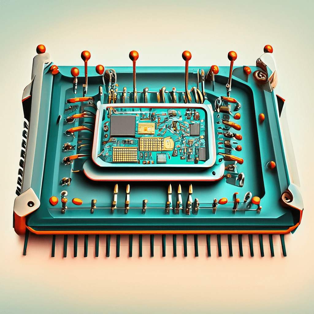
Image Generated Using Adobe Firefly
Semiconductor packaging is one of the last steps in semiconductor manufacturing and a crucial one. Protecting the silicon die from physical, mechanical, and thermal damage is only possible with a packaging solution. Silicon package technologies are also vital in developing interfaces that enable new architectures, like chiplet based XPUs.
Historically, ever since the first silicon, there have been efforts to accommodate new types of package technologies by adapting the requirements of the end application. It has been in line with Moore’s law.
Lately, one such adoption is embracing the advanced packaging technique. It is a needed solution that enables the path towards the More-Than-Moore era.
So, what does advanced packaging mean? In simple terms, advanced semiconductor packaging refers to assembly techniques developed to provide technical solutions that enable interconnections of multiple dies.
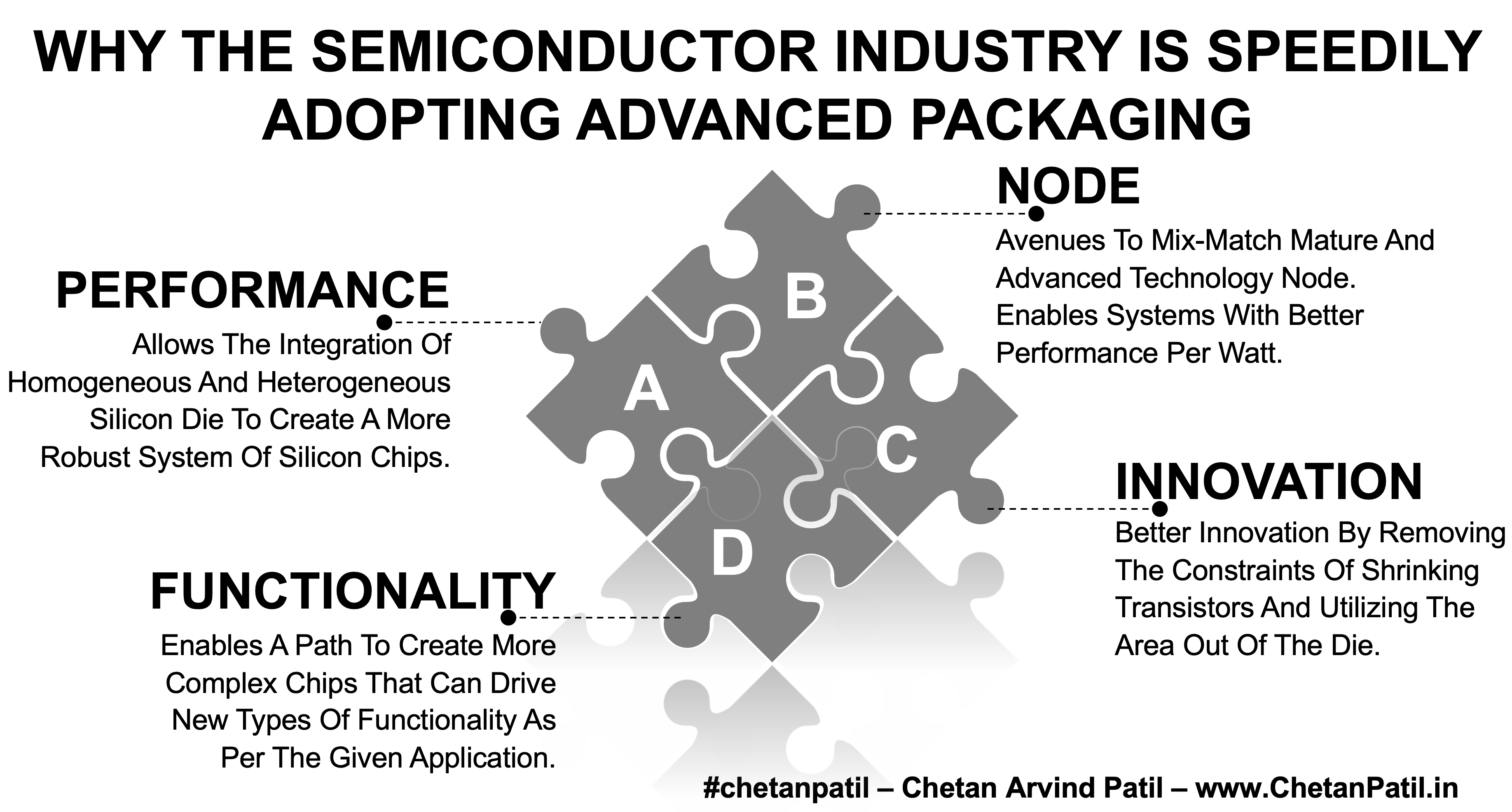
And why does the semiconductor industry need to adopt advanced packaging speedily? There are several reasons. Below are the few top ones:
Performance:
A single die and how much performance it can drive directly correlates to the physics of the semiconductor. Traditionally, it means the transistors and how fast they can shrink to double the number per the same area. Considering the ever-increasing demand for performance by the applications, it is slowly becoming impossible to cater to the advanced requirements (mainly for XPUs that are stretched to their limits by the AI applications). It is where advanced packaging comes into the picture and allows the integration of homogeneous and heterogeneous silicon die to create a more robust system of silicon chips. All of which leads to better performance.
Functionality:
Chiplet is the most talked about topic in the computing and silicon industry. The most vital aspect of chiplet is not the desegregation of the silicon die into multiple chiplets or the fabrication and testing of it, but the packaging aspect. It is valuable if the chiplets can get integrated without affecting their functionality. It is where the advanced packaging is applicable. The System-in-Package (SiP) solution is one such example of advanced packaging. It allows better integration of multiple dies and suits SoCs utilizing ultra-advanced nodes.
Node:
Advanced packaging provides the ability to keep utilizing the matured process nodes. It is to be done mainly through chiplets, which offer the ability to integrate the latest and matured nodes and then use advanced packaging to enable better node utilization, which means not having to rely on one specific technology node.
Innovation:
One of the most critical impacts of advanced packaging is to enable new silicon design. Whether by utilizing 2D, 2.5D, or 3D integration, advanced packaging provides an avenue to innovate that is not limited to die-level innovation. With advanced packaging, it has become possible to develop better integration techniques to overcome the limit of space-constrained die.
While there are benefits to embracing advanced packaging solutions, it also comes with its challenges.
The major challenge is for the semiconductor assembly vendors, who must invest the capital to develop facilities that can enable such advanced integrations and consistently develop process features to ensure the end cost is ROI-friendly.
With Moore’s Law’s diminishing returns regarding cost and performance benefits. Advanced packaging is here to play a crucial role in continuing the evolution of semiconductor capabilities and meeting the demands of new-age computing systems.
Advanced packaging addresses both technological challenges and market demands by allowing for improved performance, functionality, node utilization and driving innovation. Thus, it has become a solution that semiconductor assembly vendors are rushing to develop, and the foundries are getting into it.
The next few years will likely see the most activity in this domain and can provide a new trajectory for the semiconductor assembly industry.


