Photo by Christopher Bill on Unsplash
Advancements in package technology are as vital as advancements in technology nodes. These two semiconductor solutions enable silicon products to work per the required specifications. Technology node innovation has occurred more rapidly than package technology. Given that now the technology node is going to hit the node wall, it is time for package technology to provide avenues to shape the future of next-gen silicon design and manufacturing.
The semiconductor package has always been an integral part of semiconductor manufacturing. It has shaped and powered different silicon features and cost-optimized solutions for several decades. Semiconductor package technologies also ensure that the end-product can withstand harsh operating conditions by managing different thermal, chemical, physical and mechanical characteristics.
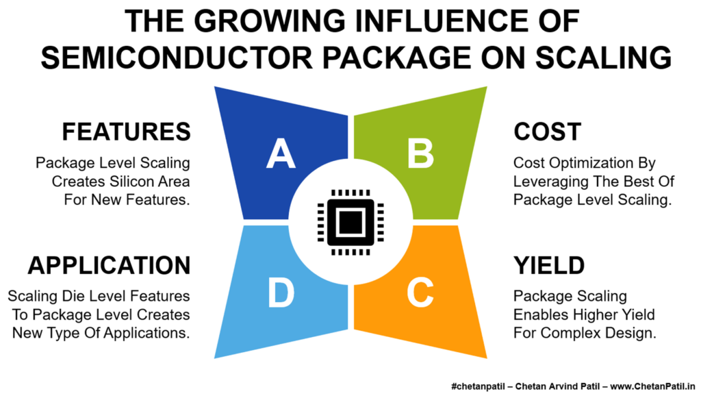
Features: Package level scaling creates silicon area for new features.
Cost: Cost optimization by leveraging the best of package level scaling.
The focus on package technologies has further grown in recent years. The primary reason is the diminishing die-level scaling opportunities, which raises questions on how the next era of silicon devices will evolve in size, shape, feature, efficiency, and performance. The answer lies in the semiconductor package evolution.
For the last decade, semiconductor package technology has consistently shown the ability to spread the die-level blocks across the different layers with the help of connections via industry-standard interfaces. It provides avenues to continue scaling for high-performance die blocks and thus deliver higher than ever capabilities.
The impact of such solutions from the semiconductor packaging world is evident in heterogeneous architectures like chiplets, and the influence of such packaging qualities will grow in the coming years.
Scaling beyond a certain point, at the die level, is complex and error-prone. It is also getting costlier and time-consuming to keep enabling die-level optimization to package more devices for better features and performance and thus pushes the industry toward package-driven scaling features.
The advanced package technology to enable scaling allows better yield. On top, the risk of introducing errors is far less than other scaling options.
Yield: Package scaling enables higher yield for complex design.
Application: Scaling die level features to package level creates new type of applications.
Apart from the yield, taking advantage of new types of packaging solutions also provides routes to design and develop new applications. It is evident from the powerful and portable solutions package technology-driven chiplet has started to enable. Similarly, different types of flip-chip solutions will soon power next-gen applications that will be far more efficient than what is available in the market today.
The influence and impact of package technology are only going to grow further, and it has already become a crucial pillar in enabling next-gen devices. Semiconductor companies which incorporate the best of both die and package level scaling will eventually be able to launch better products.


