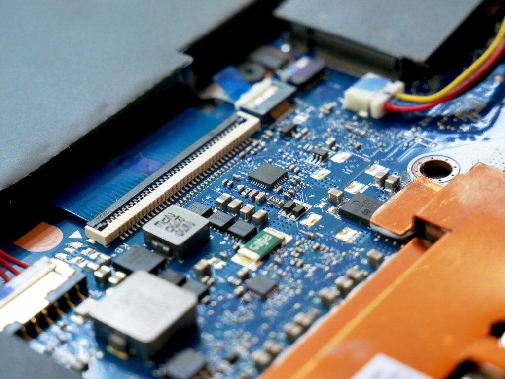
Photo by Vishnu Mohanan on Unsplash
Several semiconductor industry-wide roadmaps are planned and released by semiconductor companies and also different technical semiconductor groups. These semiconductor roadmaps are vital in providing glimpses of future semiconductor technologies and how they will shape silicon products.
Out of all the semiconductor roadmaps, the two most critical are the die roadmap and the package roadmap. These two roadmaps are drafted by separate technological groups apart from different roadmaps from semiconductor companies. There is no question that these roadmaps provide a way to design and manufacture next-gen silicon products to transform industries relying on semiconductors.
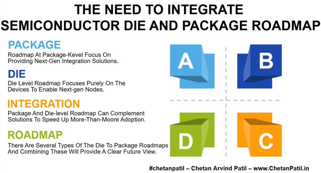
Package: Roadmap at package-level focus on providing next-gen integration solutions.
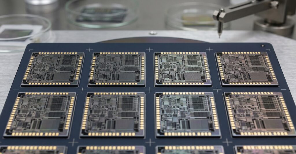
Die: Die level roadmap focuses purely on the devices to enable next-gen nodes.
However, today, the semiconductor industry is at the cross-section where the die and package solutions complement each other. In doing so, these two semiconductor technologies are pushing the semiconductor industry to adopt More-Than-Moore solutions. This intersection of technology and business goals should be the primary reason the semiconductor industry should find an integrated roadmap to provide a clear view of die and package solutions that can come together to provide more advanced solutions than ever.
Combining die and package-level roadmaps will also allow faster development of support systems. One example is chiplets, which need universal standards to combine die and package-level components to provide robust, economical, and industry-friendly More-Than-Moore solutions.

There is no denying that individual die and package-level roadmaps have sections that focus on solutions to provide a common technological platform. Even then, when it comes to implementation, several bottlenecks are present in the design to manufacturing stages. These bottlenecks range from technical (standards, yield, material, etc.) to business issues (cost, capacity, etc.). An integrated roadmap with a focus on how the industry can overcome these challenges is needed.
An integrated roadmap can also provide a clear view to enable flawless integration of next-gen die and packages to drive faster adoption towards the More-Than-Moore era.
Integration: Package and die-level roadmap can complement solutions to speed up More-Than-Moore adoption.
Roadmap: There are several types of the die to package roadmaps and combining these will provide a clear future view.
Advancement in die and package-level solutions will continue for decades. Also, the need to stack dies and packages to provide integrated solutions for the architectures like chiplets and flexible electronics will continue to rise.
Thus, for the angstrom era and the long-term innovation in the semiconductor industry, faster adoption of integrated design and manufacturing approaches for the die and package scaling will be crucial. Achieving this goal will require continuous work on an integrated die and package roadmap.


