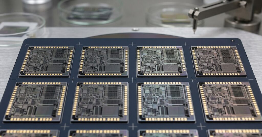
Photo by Denys Nevozhai on Unsplash
Advanced semiconductor package technologies have always played a crucial role in transistor scaling. It is also the primary reason these two scaling methods complement each other to enable customers (and industry) with innovative solutions.
Die and package level innovation have always provided the industry with solutions (chiplets, heterogeneous integration, big.LITTLE, etc.) that took the semiconductor design and manufacturing to a new level. Today, this synchronized work of die level-scaling with package innovation has taken the semiconductor industry towards a sub-1nm technology node.
Historically, the semiconductor industry has always focused on transistor scaling from two points of view:
Die: Shrinking the devices while not compromising on the power delivery.
Package: Package level scaling (SiP as an example) solution is used to tackle transistor scaling bottlenecks.
Similar to the die level integration, package level scaling can occur in two ways: Horizontal and Vertical. These two types have thus far played a crucial role in enabling customers with the desired form factors, and the importance will grow only.
The fundamental reason for the semiconductor industry to utilize horizontal and vertical integration is mainly due to the need to accommodate the new (driven by the market) requirements. Example: Chiplets methodology utilizes vertical integration at the die level and expands it further by moving dies across horizontal layers. Thus, bringing the best of the two worlds: die and package.
As the semiconductor industry moves forward with more advanced solutions, the need for package-level integration (similar to chiplets) will increase further.

In semiconductor manufacturing, package integration is often (in some cases testing occurs after packaging) the last step, but the crucial one. As the demand for better (and efficient) thermal and power insulation techniques increases, the need for advanced package-to-die level integration will rise.
Horizontal Integration: At the package level, horizontal integration provides a layer to all die by creating a common pathway for data and other communication.
Vertical Integration: Allows multiple die (2.5D/3D) to get stacked vertically and drives communication via a industry standard bus interface.
Opting for horizontal and vertical package integration is driven by the target solution. A device (silicon) utilizing the chiplet method is bound to have horizontal integration (with die-level vertical integration), while a standalone XPU might only rely on vertical integration.
Advanced packaging techniques are crucial for the next era of semiconductor-driven computing. Hence, the development of next-gen packages will require efforts from everyone: FAB-LESS, FAB, IDM, and OSAT. It is also what the More-Than-Moore era demands.
As the research and development of next-gen FETs continue, it will be essential to consider the package technologies that can provide an edge in semiconductor design and manufacturing.


