
Photo by David Schultz on Unsplash
Electronic Design Automation (EDA) is integral to semiconductor product development. Over the last four decades, the EDA industry has revolutionized how chips get designed, verified, simulated, and validated. During this time, EDA vendors have also adapted to different changing computing landscapes.
For example, the early use cases of EDA solutions used to be more local and then, with the advent of servers, became more remote. Similarly, EDA vendors have adopted cloud solutions for better performance and reliability.
Moving to the cloud has also enabled a more decentralized way of designing silicon chips. It provides a more secure form of developing an idea into a working software prototype. It has also streamlined how IPs are delivered, and licenses are maintained. In turn, the cloud also allows IP developers to ship the required files on the go swiftly.
As the complexity of the silicon design increases with the increase in features, the runtime of simulation also increases, and by adopting the cloud for EDA, the vendors can now provide scalable, high-performance computing, which shortens design validation and closure time.
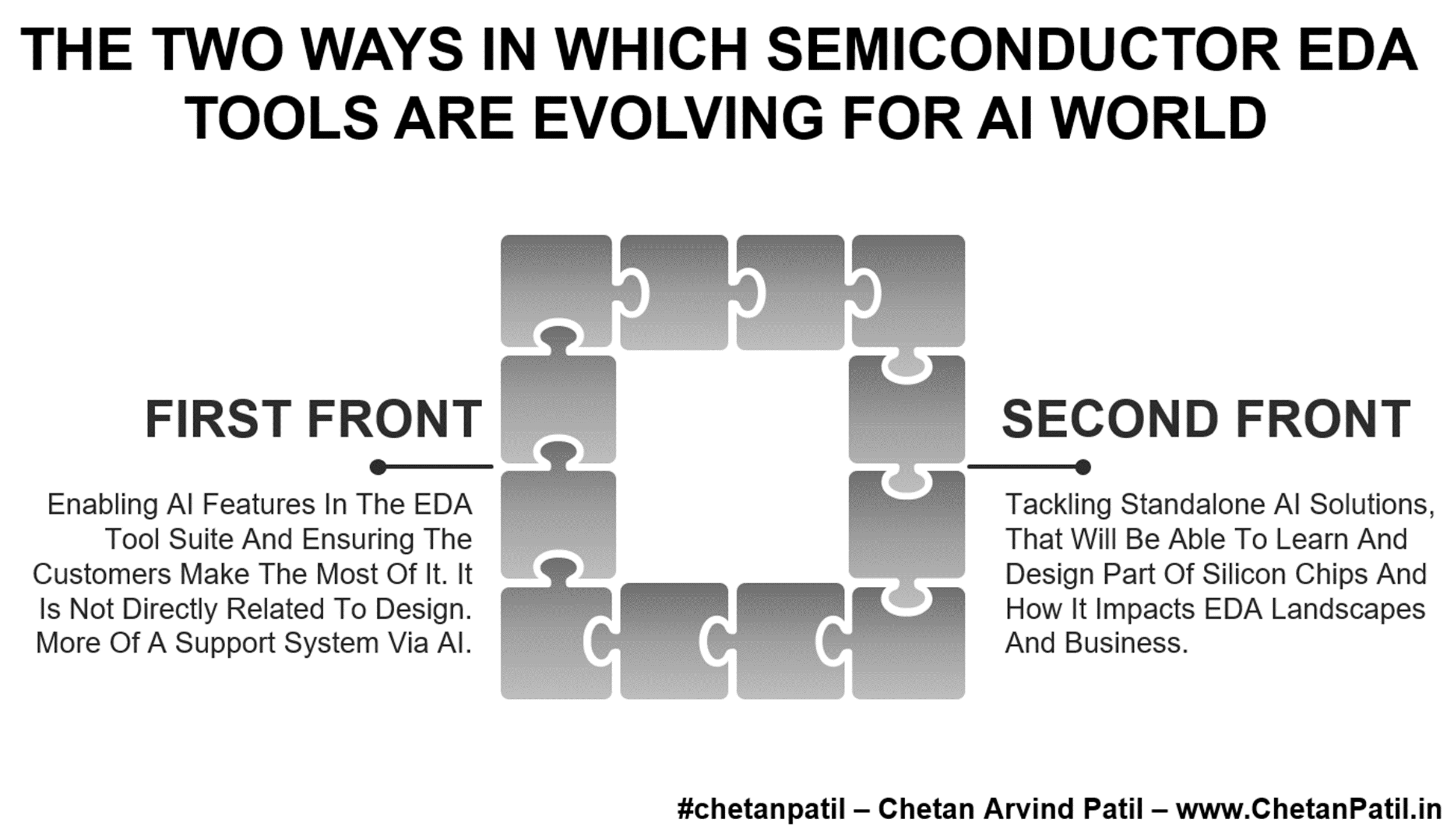
Now, the latest feature adoption for the EDA ecosystem is the AI. There are two different main ways in which EDA vendors have to accept and adopt the AI ecosystem for chip design and development:
First Front: Enabling AI features in the EDA tool suite and ensuring the customers make the most of it. It is not directly related to design. More of a support system via AI.
Second Front: Tackling standalone AI solutions that will be able to learn and design part of silicon chips and how it impacts EDA landscapes and business.
Many of the top EDA vendors have already provided the solutions on the first front. However, the second front is a tricky and new arena.
It is a space that can go in favor or against the EDA vendors. Why: If today, AI can assist in chip development, then tomorrow, what is stopping AI framework developers from creating an ecosystem?
True, this is not as easy as it sounds, and on paper, it looks fantastic, but in reality, it may be more challenging. Nevertheless, shortly, someone may create an AI framework purely for the chip designing domain to capture and learn by generating the data independently. The tricky part will be to prove the solutions, but that is where experienced semiconductor engineers will always come into the picture.
With Google, Microsoft, Amazon, and other cloud vendors moving into the semiconductor cloud EDA ecosystem, the probability of second front becoming a reality is very high, as these companies are already leading the AI front and adopting the solutions for AI self-designing chips is not going to be a tricky part.
Eventually, both fronts are new opportunities for the semiconductor EAD landscape and might open more market opportunities for EDA vendors than ever. Only time will show how these two fronts will evolve, and a lot depends upon how fast or slow the semiconductor design companies embrace AI for silicon product development.


