Photo by Christian Wiediger on Unsplash
THE IMPORTANCE OF PPA IN SEMICONDUCTOR
Semiconductor products are designed and manufactured for different conditions with varying requirements. These conditions and requirements are often a combination of several technical criteria.
One such important criteria are Power, Performance, And Area (PPA).
In the end, the goal of developing semiconductor products is to provide as much functionality possible. This requires a perfect combination of PPA: Low power consumption with high performance in the smallest area possible.
The shirking transistor size has ensured that the die/chip area is not a technical concern when designing a semiconductor chip. However, at the same time, other technical challenges are posed by small die/chip areas. Mainly, balancing the power consumption while not affecting the performance.
Three-way balancing act of power, performance, and area (PPA) is becoming more challenging when the semiconductor products are used for applications that demand lower die/chip areas while also expecting higher performance. With decreasing die/chip area and increasing performance, the management of the total power consumption (static and dynamic) also becomes an uphill task. This leaves designers with limited knobs to play with. This is why considering PPA is important when it comes to developing semiconductor products with advanced technology-node.
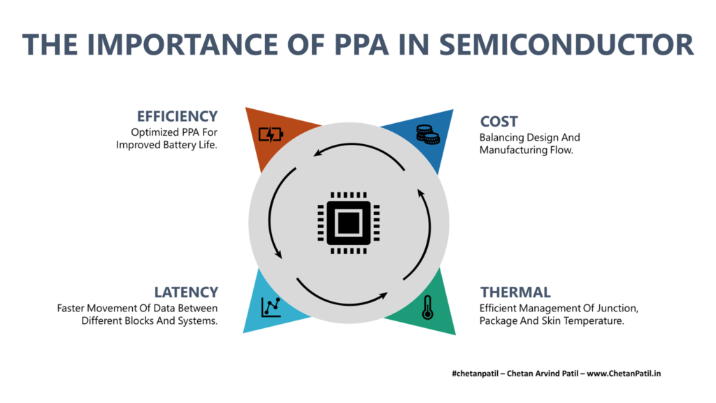
There are four major factors that PPA can have an impact on:
Efficiency: There is not a single semiconductor product that is designed and fabricated to perform tasks inefficiently. The only goal of a smart semiconductor chip is to provide maximum efficiency. While 100% efficiency is not possible, the goal of PPA is to ensure there is minimal negative impact on the battery (given majority of the electronics system run on a portable battery system), and this is achievable only when the budget (during the design phase) takes into consideration how the performance and power scheme will be for a given die/chip area. There on building the full chip design becomes a more well-laid-out task.
Latency: Larger the die/chip area the slower the data traffic. This is more valid for XPUs, where N number of cores are working in synchronization to achieve the single task of crunching the data in the faster possible time. If the area is large and the layout is not optimized, then the latency introduced will be higher. On the other side, a large area (or even smaller in some cases) also has a far greater impact on total power consumption, while the performance is mostly on the positive side. This is another reason why balancing PPA becomes a critical task in semiconductor product development.
Thermal: Smaller the die/chip area, the less room there is to transfer the heat out of the system. This also leads to more static power consumption apart from the dynamic. On other hand, smaller area also requires advanced technology nodes that eventually mean higher junction and package temperatures (apart from skin temperature). This eventually demands smart dynamic thermal management techniques, which are only possible if PPA is managed efficiently.
Cost: In the end, the goal of any product (not just semiconductor product) is to optimize the cost of development. PPA plays a crucial role in cost too. Increasing die area can mean less room for more dies on the wafer, which means more wafers to product higher volume, and this eventually leads to higher development cost. This is another reason why PPA is an important factor when it comes to increasing product margin.
At the end of the day, the ultimate goal of the semiconductor product is to provide solutions that not only fit the market but are also the best version in the given category.
This is where optimizing PPA is vital, as it ensures the different functionality of the given die/chip is geared towards a product that outperforms any other competitor in the market.
THE PPA BOTTLENECK IN SEMICONDUCTOR
Designers worldwide are always working towards the goal of achieving the required specification. This allows them to ensure that the semiconductor product is meeting all the criteria for the system it will eventually become part of. However, there are always design constraints, and PPA is one such vital constraint.
In reality, it is difficult to create a perfect balance of all the three components of PPA. One of the other parameters will always outweigh the other. This is more valid for critical semiconductor components like XPUs, which often demands less die/chip area for high performance.
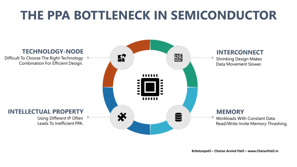
Still, there are PPA driven bottlenecks that may hinder the success of the product:
Technology-Node: Balancing PPA does require choosing chip development technology that covers not only the product’s technical requirement but is also not costly to manufacture. Post design, the technology-node is going to stay with the product till the end of the product’s life. This is why PPA can many times drive technology combination choices that may not always be advanced. This may or may not have a major impact on the product’s success, however, PPA certainly adds constraint on the choice of technology-node.
Intellectual Property: The semiconductor design is getting increasingly driven by IP. This can be a bad news for the next-gen chip design as every new IP block might already have its PPA budget/scheme. This hinders the ability to play with the chip’s overall budget/scheme. This is why IP can sometimes introduce PPA bottlenecks in the chip designing process.
Memory: Memory is one of the most critical pieces of block in any given modern chip. More so when the chip is designed for workload-intensive tasks. The unpredictable number of reads/writes can through away the PPA budget for any given product. In such scenarios, it becomes difficult to count on the PPA budget scheme and often requires millions of simulations to validate the PPA scheme. This leads to bottlenecks on the design schedule and adds pressure to validate all the possible read/write scenarios.
Interconnect: If the area component of PPA has large say in the overall budget, then it can often lead to interconnected block systems that can introduce a lot of data traffic. This can have a heavy impact on-chip performance. This is often true for XPU based semiconductor chips. This is another possible way in which PPA introduces bottlenecks into the system.
As the semiconductor industry moves towards more advanced FETs, the importance of PPA will grow too. It can either lead to PPA schemes allow chips to outperform their predecessors or it can also have a negative impact (due to unbalanced PPA schemes). This is also one of the major reasons why new FETs and silicon chips are primarily focused on PPA to showcase the positive features of their new solutions.
In the long run, as newer FETs and technology-nodes get developed, both the semiconductor design and the manufacturing process will keep dealing with the act of balancing the PPA.


