THE MOVE TOWARDS THE NEXT-GEN SEMICONDUCTOR PACKAGE TECHNOLOGY
Packaging plays an important role in almost all the industry. From cars to rovers, packaging the product before shipping is vital. Doing so cost-effectively is critical to ensure the product cost is not affected.
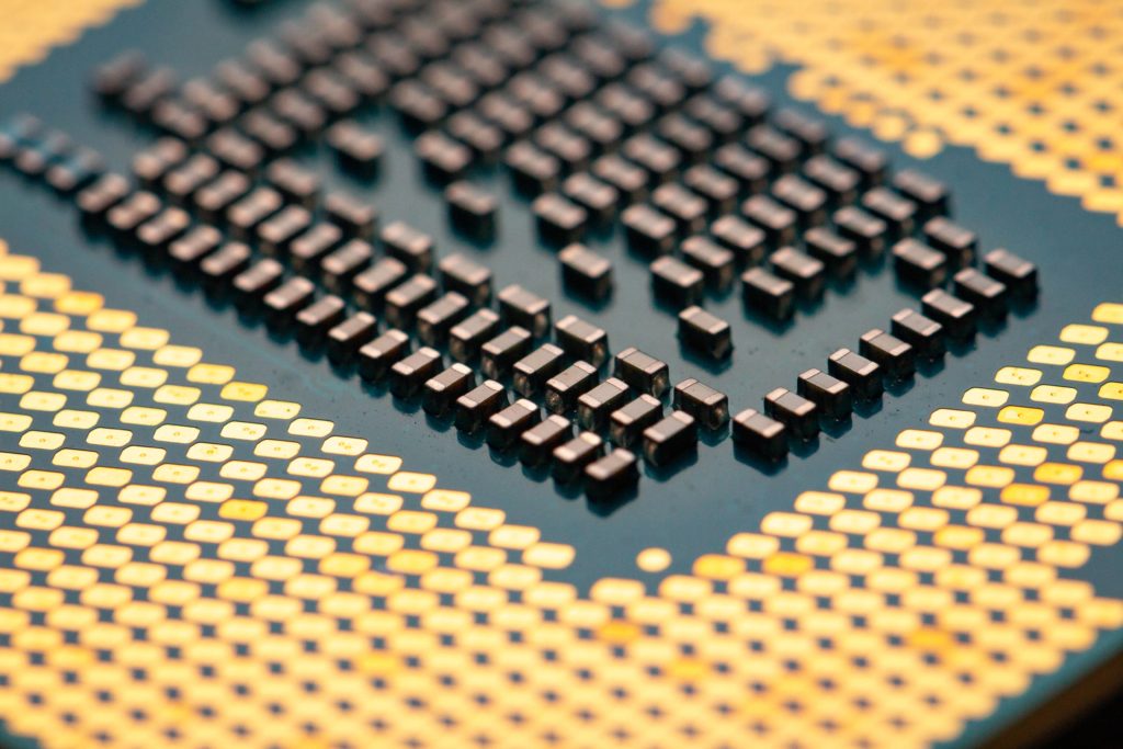
The same story is valid for the semiconductor industry, where the packaging technology ensures that the silicon die is protected from harsh mechanical to environmental conditions.
In a nutshell, package technology in the semiconductor industry is geared towards providing the following features to the die area:
Thermal: Ensure the heat is dissipated efficiently out of the die to avoid thermal runaway.
Mechanical: To save silicon from any outside impact like vibration or stress.
Connectivity: Enable a pathway for connecting the die to another system via a printed circuit board.
Contamination: Protect the die are from contamination due to long-term usage.
Today, there are numerous package technologies to choose from. Eventually, the decision to decide on the package type is based on both the technical and the business points.
Give the advancement in the semiconductor design and ever-shrinking technology-node, it is becoming a challenge for semiconductor packaging solution providers to come up with innovative packaging solutions that are also low-cost. All this is pushing the need for next-gen – InFO, CoWoS, CoC, FCiP, PoP, and many more – package technology solutions.
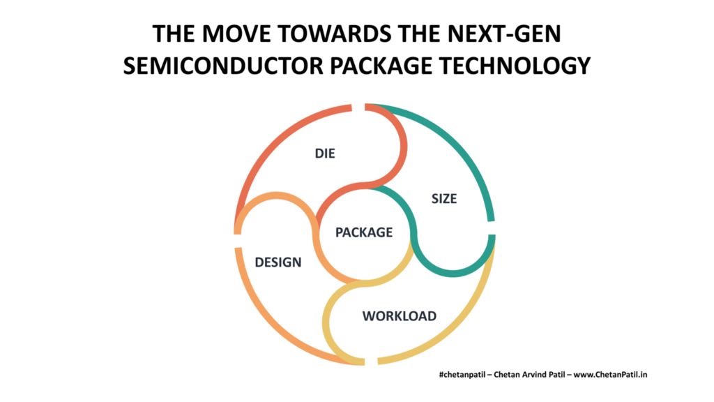
The push towards next-gen package technology is driven by several factors:
Die: Semiconductor product development is moving towards More-Then-Moore solutions. This means several new die-based solutions and one of them is chiplets. Chiplets is IP driven design process, where different die come together to form the same system which earlier would have been a single die. Chiplets are proving to be effective both from a cost and yield perspective. To cater to such requirements, package technology solution providers (OSATs) have to keep their innovation team engaged, to ensure not only the packaging solution is at-par with chiplets requirement but are also low-cost due to the stiff competition.
Design: One example of modern semiconductor design change is the heterogeneous architecture. It has provided ways to bring different types of XPU together. This also requires an efficient way to package by considering the thermal profiles of such complex and high-frequency devices.
Size: The shrinking size is also adding to the need to be more innovative in package technology. Not all devices will be small and at the same time also not too big. OSAT is facing a challenge to cater to different markets and while doing so, have to ensure the type or size of the device is not a constraint.
Workload: Emerging workloads are becoming complex year-on-year. These workloads running on the die continuously end up heating the system. To mitigate such issues, new materials and packaging solutions are required. This is also one reason that is pushing OSATs towards next-gen package technology.
OSATs have to continuously provide solutions that cater to both the smaller and larger die areas. This has to be done in coordination with the design houses, to ensure that next-gen package technology meets all customer requirements.
However, lately, OSATs are being pushed from all the corners and are getting beaten in their own game by FAB-LESS to FAB houses.
THE RACE TOWARDS NEXT-GEN SEMICONDUCTOR PACKAGE TECHNOLOGY
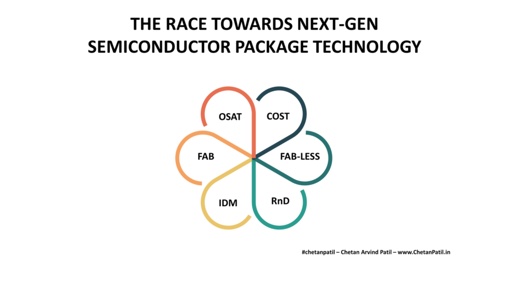
The semiconductor package technology is mostly enabled by the OSATs. IDMs also play a crucial role. However, given the rise of the semiconductor packaging and testing business, OSATs are facing stiff competition from FAB and FAB-LESS companies too.
This is leading to both positive and negative impact on all types of semiconductor companies:
OSAT: The primary focus and strength of the OSATs have been the testing and packaging solutions. With growing competition from FAB on the packaging solutions is certainly putting OSAT in a position to not only innovate on the testing to packaging arena but also how to expand the business beyond traditional OSAT services. This certainly diverts the focus of OSATs, as it is more difficult to move towards FAB or FAB-LESS business while also catering to the same customer type.
FAB: FABs all over the world have the biggest advantage due to the availability of high-tech and research facilities that can aid the innovation of next-gen package technology. This is why TSMC and Samsung have been at the forefront of next-gen packaging solutions. At the same time, FABs are also diversifying and entering the OSAT business with a strong packaging portfolio.
IDM: IDM has always enjoyed the best of both world. Intel already has many homegrown packaging solutions for its need, apart from the ability to fabricate, test and assembly in-house. The innovation in the design space is only benefitting IDMs as they can foresee and quickly adapt their business by pushing towards the required semiconductor packaging research and development activity, and quickly turn research into production-worthy solutions.
FAB-LESS: While, majority of the FAB-LESS companies only focus on the design side. The need to have a packaging solution that can cater to their designs is also pushing FAB-LESS to continuously invest time and money in the packaging technology.
Eventually, packaging solution for semiconductor products is driven by cost optimization. The innovative and low-cost packaging solution catering to the next-gen design will win the race. However, to do so massive research and development activity is required. Which certainly demands high CapEx.
To balance the complexity and high CapEx, packaging solution providers (OSATs mainly) will have to be more innovative to ensure the next-gen solution is business-friendly.
The race towards next-gen semiconductor package technology is certainly heating up, however, it is also an opportunity to innovate and create a new market for the emerging solutions.


