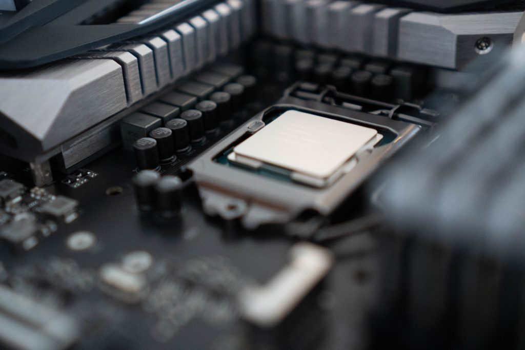
Photo by Luan Gjokaj on Unsplash
OVERVIEW
Computers are designed to provide real-time feedback to all user requests. To enable such real-time feedback, Central Processing Unit (CPU) is vital. CPU is also referred to as processing units or simply processors. These incredibly small semiconductor units are the brain of the computer and are capable of performing Millions/Billions of Instructions Per Second (MIPS/GIPS). High MIPS/GIPS, means faster data processing.
A lot of processing goes on inside these processing units. With the advancement of the technology nodes, more processing units are being glued together to form System-On-A-Chip (SoC). These SoCs have different individual units like GPU, DRAM, Neural Engine, Cache, HBM, ASIC accelerators, apart from the CPU itself.
It is incredibly difficult to design an SoC that has the best of two important worlds of computer architecture: Power and Performance.
Both in academia and the industry, Computer Architects (responsible for design and development of next-gen CPU/SoC) play a key role and are often presented with the challenge of understanding how to provide faster performance at the lowest power consumption possible. It is a difficult problem to solve.
The battery technology has not advanced at the speed at which SoC processing capability has. Shrinking technology node offers opportunities to computer architects to put more processing power, but at the same time, it also invites issues related to the thermal and power budget.
All this has lead to semiconductor companies focusing on design challenges around the power and performance of the SoC.
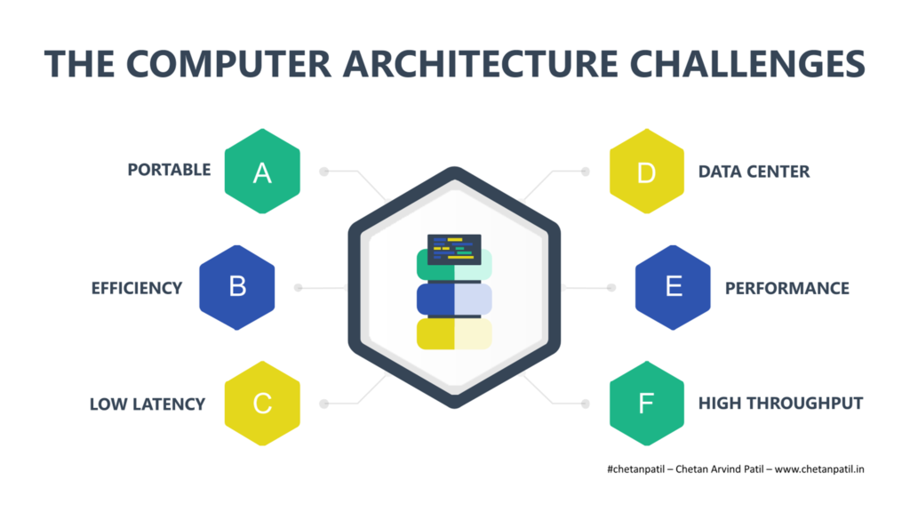
CHALLENGES
Semiconductor industry has been focusing on two major SoC design challenges:
- Challenge 1: Efficient and low latency SoC design for portable devices
- Challenge 2: High throughput and performance oriented SoC for data center
Challenge 1:
- Portable:
- Portable devices suffer from the constraint on the battery capacity. The battery capacity has been increasing mainly due to the shrinking board inside these devices due to the shirking transistor size.
- This has allowed the OEMs to put more lithium-ion. However, to balance the form factor and portability, batteries cannot be scaled out forever. It is a challenge for OEMs to understand how to manage portability by balancing the battery size apart from making the computer system efficient with low latency.
- Efficiency And Low Latency
- To tackle efficiency and low latency, innovative designs are coming out in the market with the ability to adapt the clock and voltage domain depending on the application being executed by the user. It is no more about how many cores are in the SoC, but more about how an application-specific core can provide a much better user experience than ever.
- This has presented researchers with an interesting problem of improving the performance per watt (PPW). To improve PPW, researchers around the globe are taking different approaches around DVFS schemes, apart from improving transistor level techniques.
- Frequency and voltage level scaling also has a direct impact on the response time. Processing units like CPU are designed to provide low latency so that all the request coming in, can be catered to in real-time.
- Improving efficiency without compromising on the latency is still a big challenge for the computer architects.
Challenge 2:
- Data Center:
- On the opposite pole, data centers are designed to be compute-intensive. The SoC required to cater data center has exactly the opposite need compared to portable devices. As companies become data aggregators, the analysis requires dedicated hardware that provides streamlined computation of the data on the go.
- This is prompting companies like Google, Facebook, and Amazon to come up with their silicon that understands the data being generated and how to swiftly analyze it on the go.
- Performance And High Throughput:
- Designing custom SoC requires a fresh look and is drastically different than the block based approach. Improving throughput requires high speed interconnect to remove bottlenecks in data processing, else the performance will be affected.
- In order to improve throughput, the data needs to reside near the computation block. This demands a new way to predict data to be used in order to bring in the cache or add a memory hirerachy with the help of MCDRAM.
The challenges are many and researchers around the globe are already working to provide elegant computer architectures both from academia and the industry.
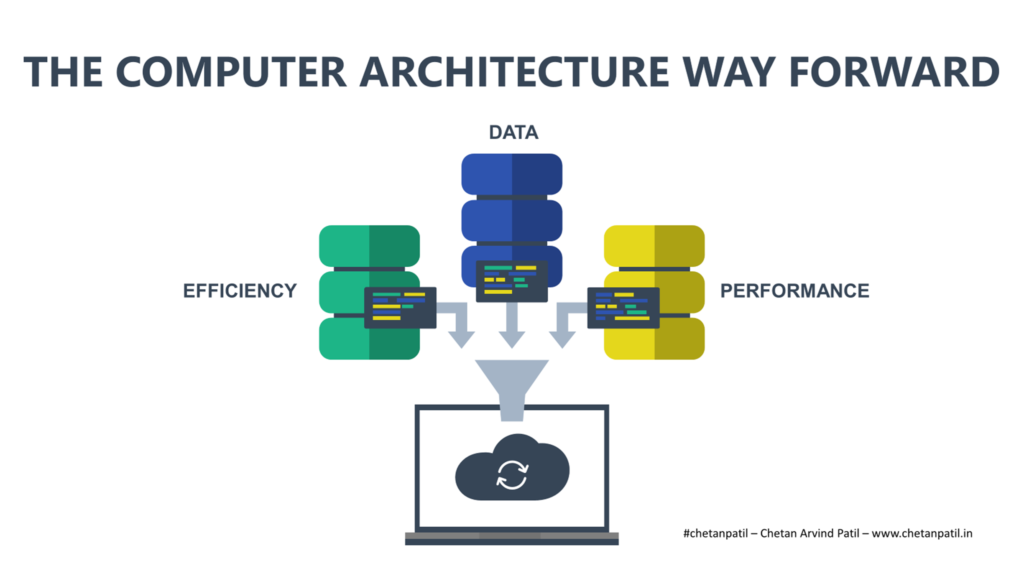
WAY FORWARD
As the need of the application running on the computer systems is changing, so is the approach to designing SoC. Various examples from different companies show how the development of computer architecture is changing and will eventually help others come up with new computer architectures.
These new architecture designs are taking the traditional approach of computer architecture and providing a different way to tackle both memory and compute bottlenecks.
Cerebras came up with Wafer-Scale Engine (WSE), which is developed on the concept of fabricating full wafer as a single SoC. The performance data of WSE show a promising future of how computer architecture becomes more wafer-level designing than die level. WSE also takes different approach on interconnects by utilizing wafer scribe lines to transfer data which provide more bandwidth.
Fungible’s Data Processing Unit (DPU) architecture is another way forward that shows how SoC will be increasingly get designed for scale-out systems to handle massive data.
Google’s TPU and Amazon’s Inferentia shows how custom ASIC based SoC will become de-facto. Companies that generate a lot of data will try to run their center on in-house developed SoC.
Apple’s M1 launch showed how ARM will start eating the x86 market for energy-efficient portable devices. In few years, the integration will become more intuitive and might attract other x86 portable devices OEMs who have failed to take Windows on ARM to its true potential.
NVIDIA’s bid to acquire ARM shows that the future GPU will be designed with a blend of fusion technology that will combine ARM/CPU with GPU more than ever. This will allow data centers to improve on latency apart from focusing on throughput.
In the end, all these are promising development for the computer architecture community. Provides numerous opportunities to research and develop new ways to enable lower latency and higher throughput while balancing power consumption.


