Photo by Dan Cristian Pădureț on Unsplash
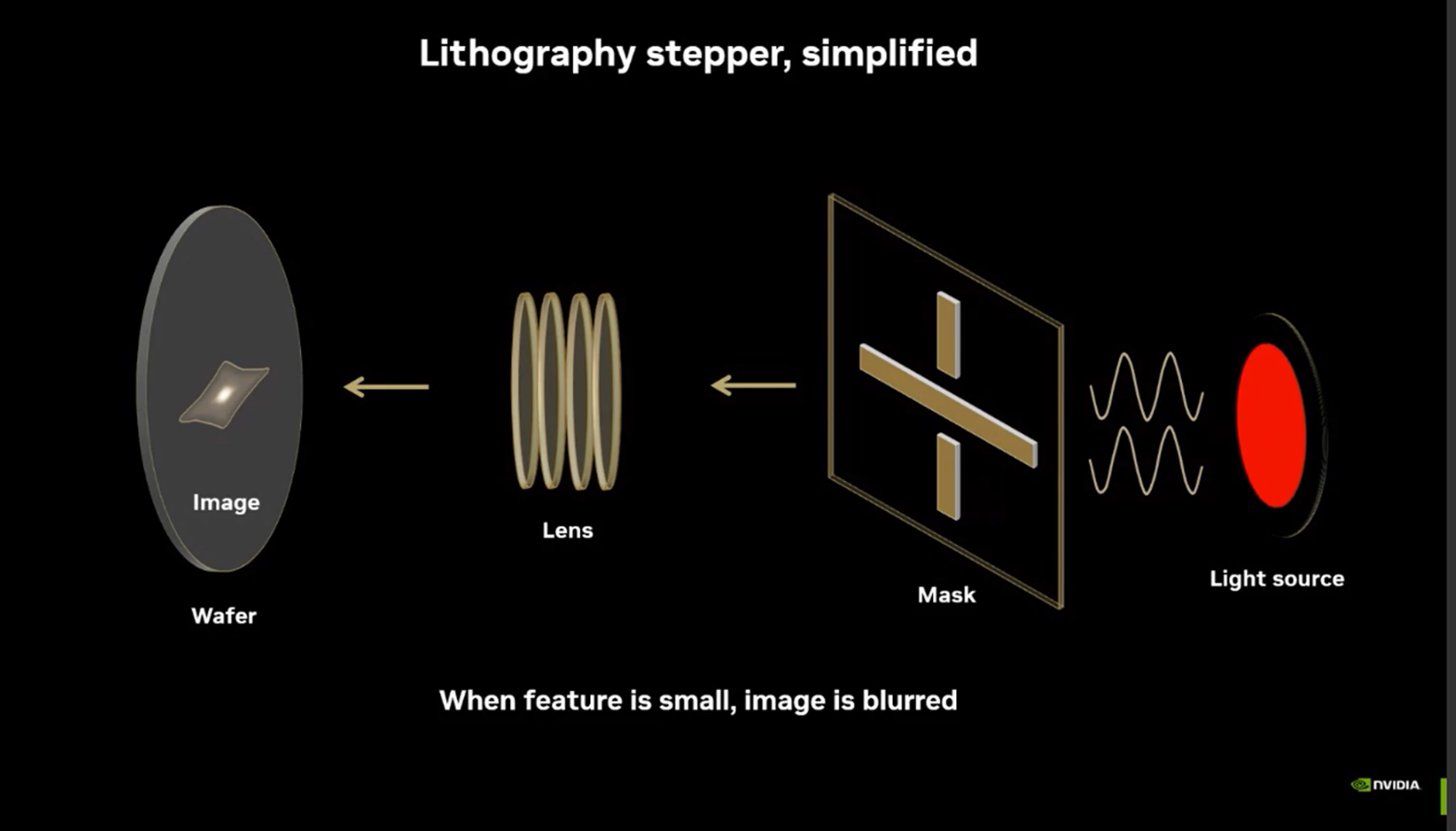
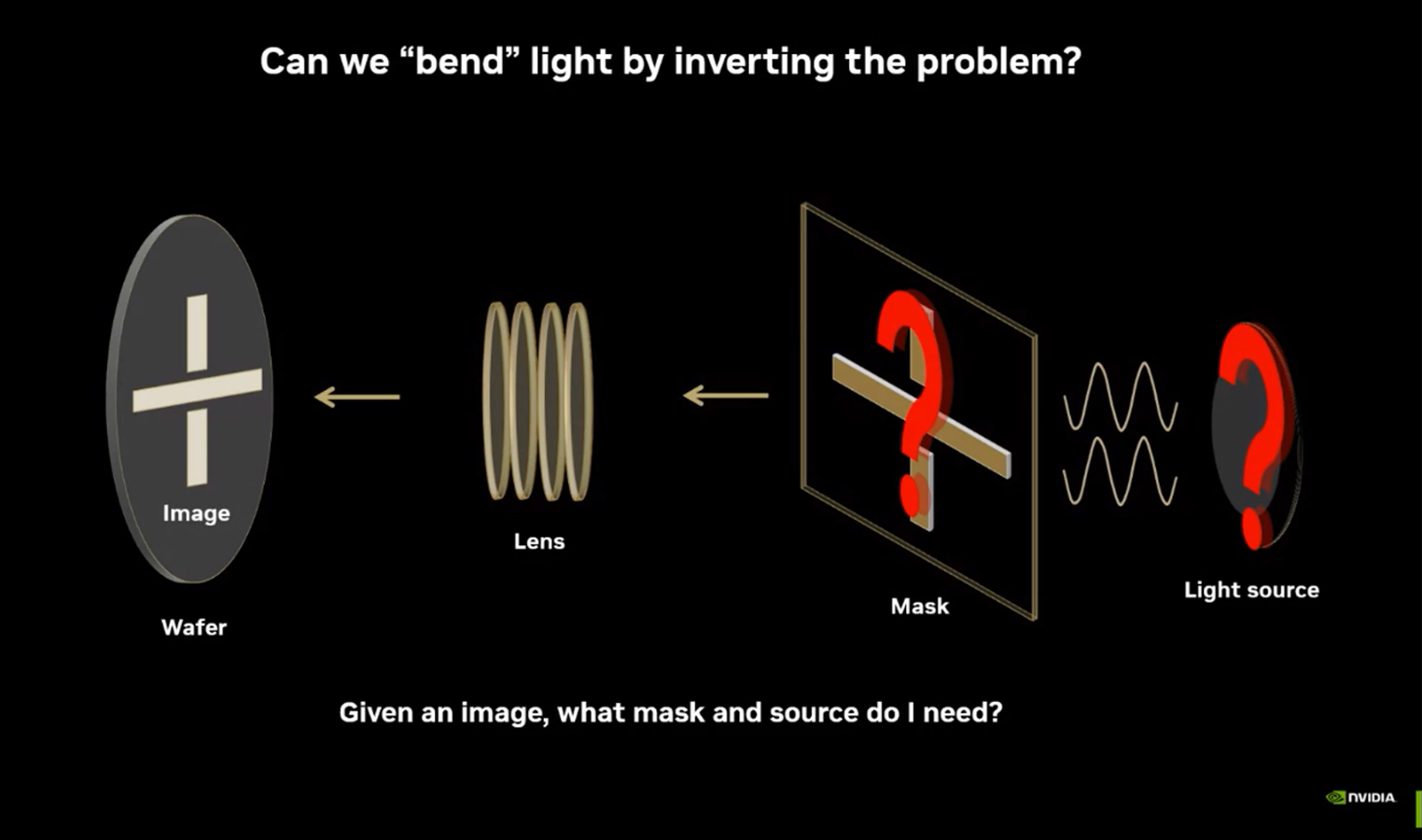
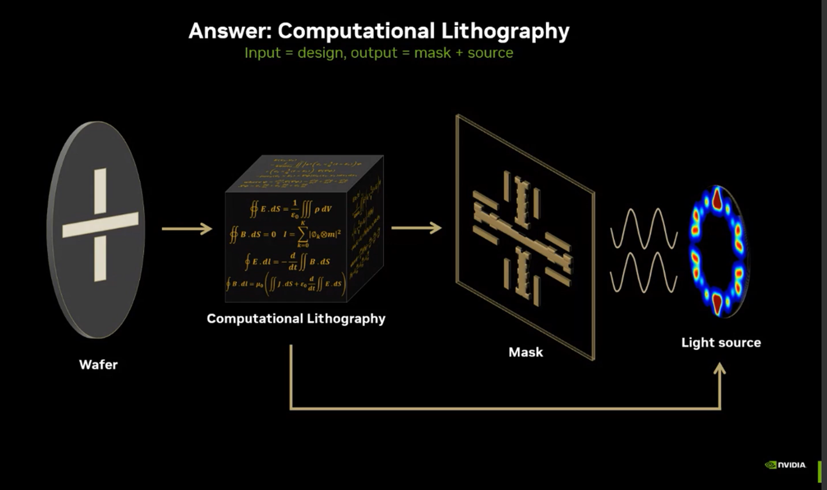
Computational lithography is a specialized field in the semiconductor manufacturing domain. It is used during lithography when advanced algorithmic models optimize the patterning and masking process. It is done by deforming the patterns to compensate for the physical and chemical effects naturally occurring in a standard flow. It utilizes the concept of inverse lithography to do so.
Result: Accurate production of the desired chip patterns on the wafer to fabricate the complex advanced node silicon.
Achieving such a complex and exact process on the go demands compute speed. It means that the equipment must either be equipped with high-performance XPUs to deliver a modeling approach or be able to offload and on load. In practice, the remote and distributed processing approach is better suited.
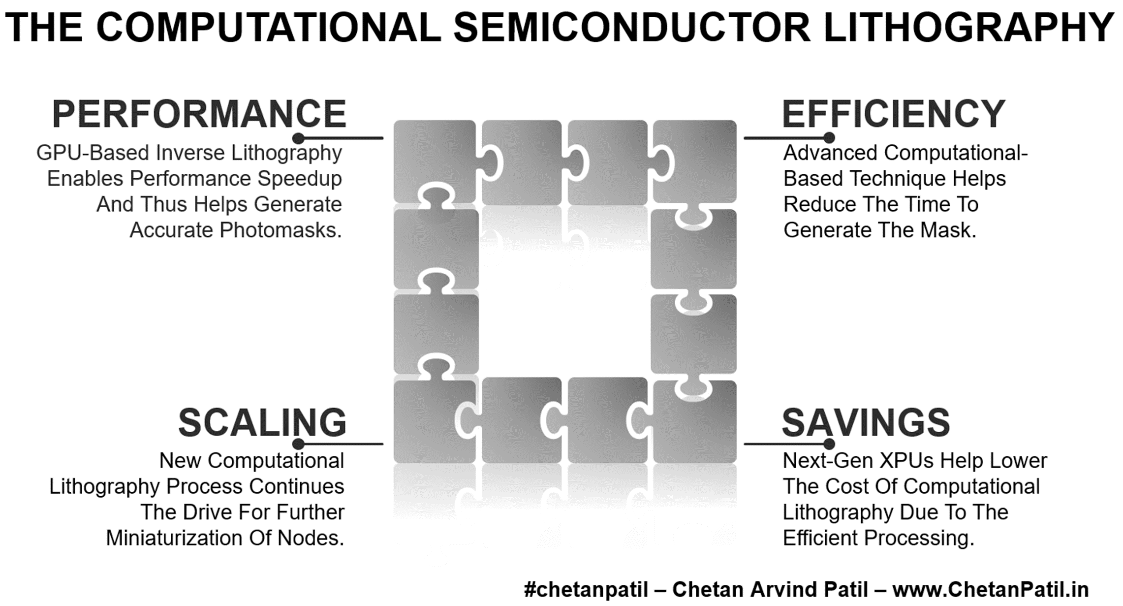
Performance: GPU-based inverse lithography enables performance speedup and thus helps generate accurate photomasks.
Efficiency: Advanced computational-based technique helps reduce the time to generate the mask.
However, as the complexity of the technology node increases, it has become challenging to keep up with the processing requirements of lithography. Thus, better XPUs and also software support is required.
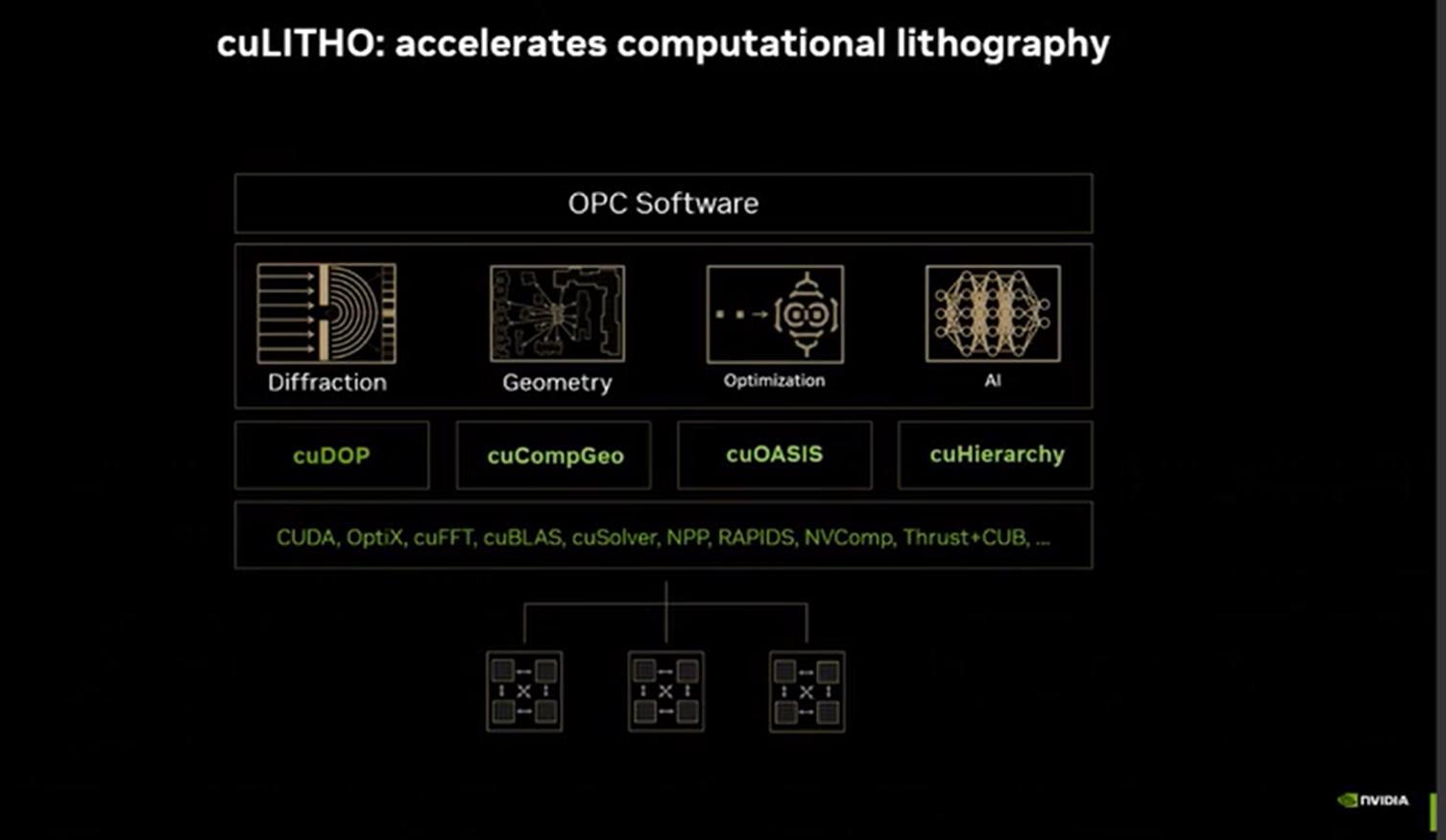
To tackle this bottleneck, NVIDIA, Synopsis, TSMC, and ASML have collaborated to leverage the software libraries on the GPU architectures. It will help drive silicon scaling and enable their end users to reduce costs and accelerate technology advancements. It leverages GPU-based inverse lithography.
Below is a simplified flow of what this collaboration will speed up further. Details around the litho library (cuLitho) were presented by Vivek K Singh, Vice President, Advanced Technology Group, NVIDIA, early this year.
It is a significant step in the right direction when there is a proper set of collaborators: Covering GPU, EDA, Technology-Node, and Semiconductor Equipment experts.
Today, the compute workloads that achieve computational lithography are the most complex and extensive computational activity ever executed during semiconductor production.
Savings: Using next-gen XPUs help lower the cost of computational lithography due to the efficient processing.
Scaling: New computational lithography process continues the drive for further miniaturization of nodes.
With the latest advancements in GPU technology and the collaborative approach, computational lithography performance will skyrocket.
Eventually, semiconductor manufacturers will now achieve unprecedented speed and accuracy for all the lithography requirements. Such an improvement will also help drive better die-level manufacturing accuracy, improved yield, and the ability to continue to scale into the Angstrom era.


