RECENT BLOG Post

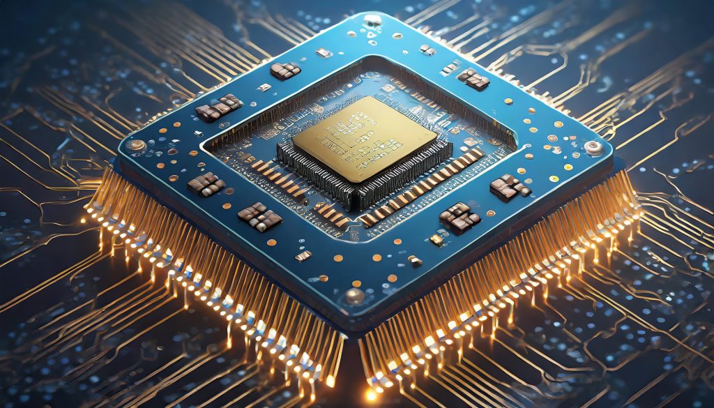
Adobe Firefly Several companies have established themselves as prominent mobile System-On-A-Chip (SoC) technology players. The landscape is characterized by

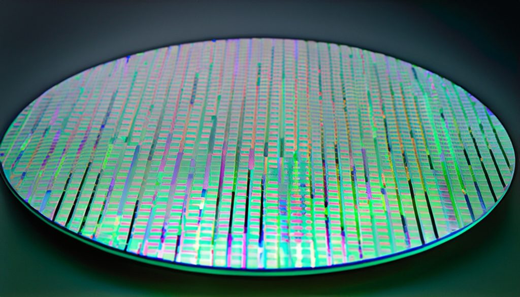
Adobe Firefly In semiconductor manufacturing, lithography is a pivotal process. It involves transferring circuit patterns onto a silicon wafer,

Adobe Firefly Graphics Processor Units (GPUs) have become the default go-to architecture whenever the requirement is for faster throughput.

Adobe Firefly What Is Semiconductor Yield Management: The manufacturing of semiconductor devices is a highly intricate process that involves
Adobe Firefly The realm of artificial intelligence (AI) is experiencing a transformative shift, primarily driven by innovative AI chips

Adobe Firefly Semiconductor test engineering is a specialized domain within the semiconductor industry that ensures integrated circuits (ICs) function
Adobe Firefly Semiconductor wafer processing is an intricate series of steps to produce integrated circuits on silicon wafers. Artificial

Adobe Firefly Semiconductor packaging is one of the last steps in semiconductor manufacturing and a crucial one. Protecting the
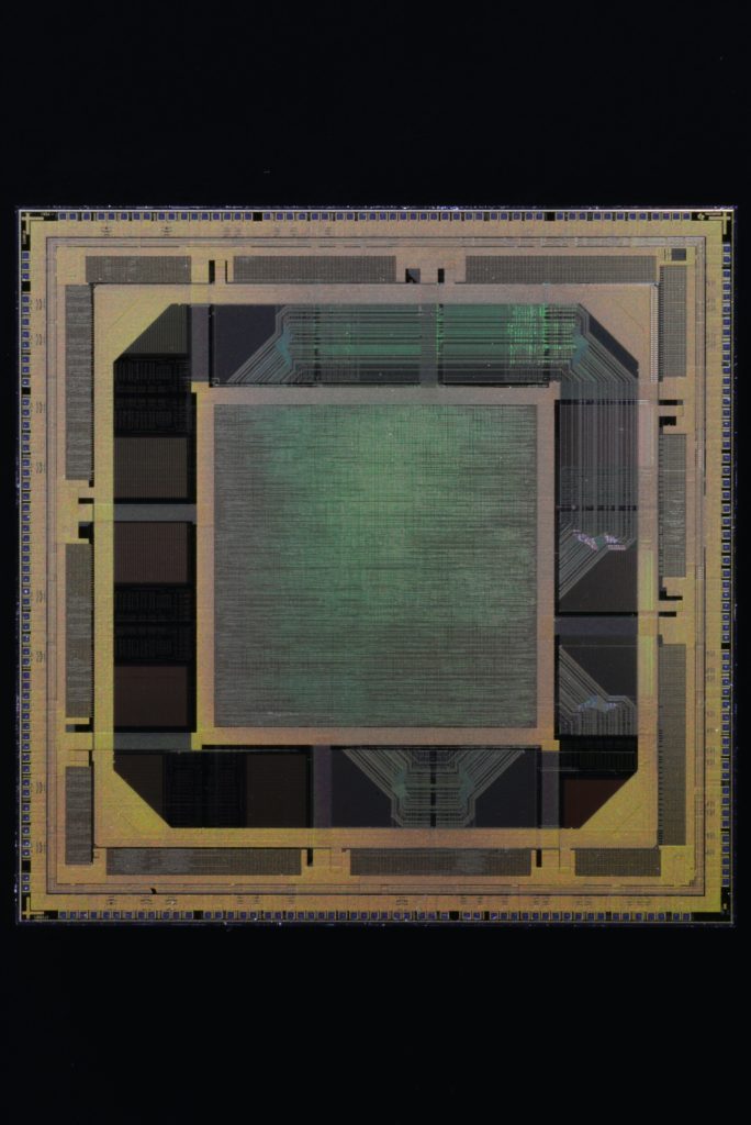
Photo by Laura Ockel on Unsplash Chiplet is undoubtedly the most suitable semiconductor design and manufacturing solution to scale complex