The Semiconductor Lithography Race: NIL VS EUV
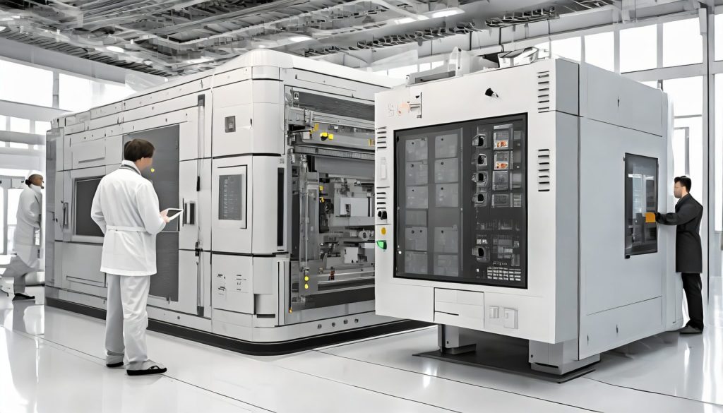
Adobe Firefly In semiconductor manufacturing, lithography is a pivotal process. It involves transferring circuit patterns onto a silicon wafer, a foundational step in creating integrated circuits (ICs). Two of the most advanced lithography techniques currently at the forefront of this industry are Extreme Ultraviolet (EUV) and Nanoimprint Lithography (NIL). Nanoimprint Lithography (NIL) and Extreme Ultraviolet Lithography (EUV) are two technologies used in semiconductor fabrication, each with advantages and challenges. Below is a comparative analysis. Extreme Ultraviolet Lithography (EUV): Technical Overview: EUV lithography employs a highly sophisticated process that uses extreme ultraviolet light (with a wavelength of approximately 13.5 nm) to etch wonderful patterns onto silicon wafers. This technology is a leap from traditional lithography, which uses deep ultraviolet light. Advantages: The primary benefit of EUV is its […]