
Image Generated Using Adobe Firefly
What Is Semiconductor Yield Management:
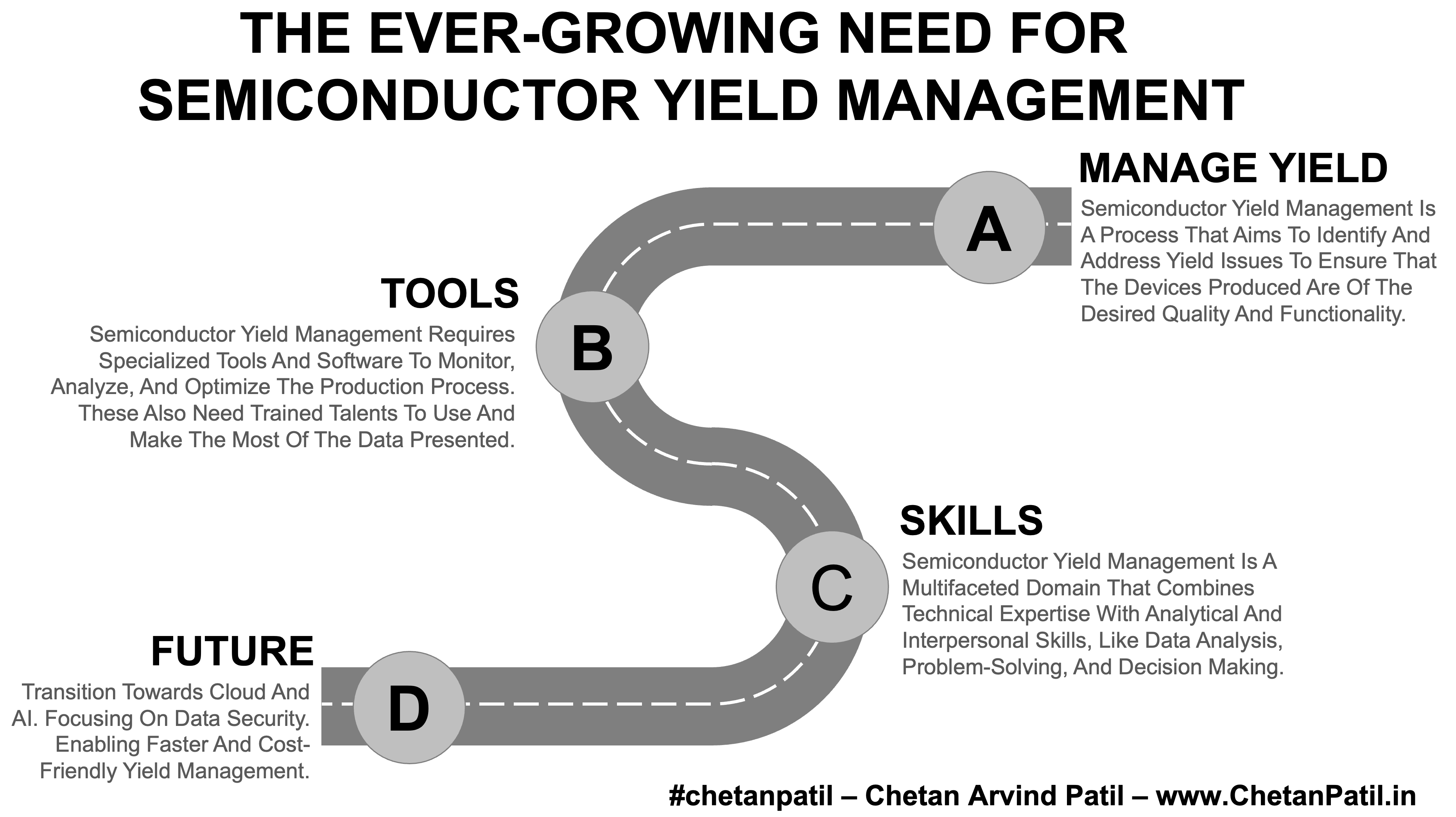
The manufacturing of semiconductor devices is a highly intricate process that involves multiple steps. Even minor deviations in these steps can result in defects that render the device non-functional. Semiconductor yield management is a process that aims to identify and address yield issues to ensure that the devices produced are of the desired quality and functionality. Its main goal is to maximize yield by minimizing the number of defective devices and optimizing the manufacturing process for better productivity.
Often, yield management is assumed to be only about silicon test data. In reality, it is much more than that. It is about ensuring all the process steps from wafer start-up until the final packing stage is equipped with a yield monitoring process
How Is Yield Managed In A Semiconductor Production Flow:
Semiconductor yield management requires specialized tools and software to monitor, analyze, and optimize the production process. These also need trained talents to use and make the most of the data presented.
As an example, defect inspection tools help to scan wafers at various stages of the process steps. It allows the detection of physical defects. Similarly, Scanning Electron Microscopes (SEMs) provide high-resolution imaging to detect and analyze weaknesses that are not possible due to defect inspection tools – mainly as part of failure analysis.
At the testing stages, a flawless yield management software that can work synchronously with Automated Test Equipment (ATE) to capture, process, and analyze vast amounts of data is needed. This end-to-end data is crucial in ensuring the yield out of the wafer is in line with the specification, and YMS tools offer various features to facilitate the review process that may arise due to any excursions or issues during testing.
In line with YMS, there is Statistical Process Control (SPC) Software, too, that ensures in real-time, the process remains within specified limits. On top of that, many of the SPC tools have different types of rules that can capture test-driven deviations in real during silicon wafer testing.
Human Skills Needed for Semiconductor Yield Management:
Semiconductor yield management is a multifaceted domain that combines technical expertise with analytical and interpersonal skills. Some of the top-level skills a talent needs to have are:
Analytics: Yield management is analyzing large amounts of data to identify patterns, anomalies, and potential causes of defects. Professionals in this field must be skilled in dissecting data, using statistical tools, and deriving actionable insights from complex datasets. Additionally, having the ability to write automated tools in various programming languages is an added advantage.
Focus: Manufacturing semiconductors involves thousands of intricate steps, and even the slightest deviation can lead to defects. It is essential to possess a keen eye for detail to identify and rectify minute discrepancies that others might overlook. Additionally, understanding different sets of fabrication process steps and how to connect the anomalies is also crucial for ensuring a successful outcome.
Problem-Solving: Yield management professionals must quickly diagnose and resolve issues during the production process, using a structured approach to creative problem-solving.
Communication: Interdisciplinary teams of yield management professionals must communicate effectively to relay findings, suggest improvements, and ensure corrective measures are implemented. It is like a decision review system (as in Cricket), where the solution goes through a review before it gets deployed.
Collaboration: Yield improvement is a collective effort. Collaboration among professionals from various functions is crucial for yield improvement.
Decision: With the vast data, yield management professionals must make timely and informed decisions, balancing the trade-offs between quality, cost, and production speed.
Transition Towards Cloud, AI, Hurdles And Future:
Traditionally, the semiconductor end-to-end data analysis is not only challenging to capture (due to disaggregated tools and equipment) but is also costly. The costly aspect is due to the need to deploy a proper set of hardware and software systems that can provide end-to-end data capturing.
So far, many yield management flows in the semiconductor industry have yet to adopt the cloud and AI strategy. And, with AI usage increasing, it has become crucial for semiconductor companies to not only embrace AI solutions but also move or adopt cloud solutions to ensure the AI features can be developed at scale, as both go hand in hand.
Cloud: With the increasing complexity of semiconductor designs and processes, the amount of data generated during manufacturing has grown exponentially. Cloud platforms offer vast storage capabilities and enable seamless access to data across global manufacturing sites. This centralization facilitates real-time data analysis and quicker decision-making. Semiconductor engineers and data scientists from different locations can simultaneously analyze data, discuss findings, and implement solutions, ensuring that yield optimization strategies are consistent across facilities.
Art Of AI: AI algorithms can predict potential yield issues based on historical data. This proactive approach allows manufacturers to address potential problems before they manifest, ensuring higher yields. Traditional methods can be time-consuming. AI can quickly sift through vast datasets to pinpoint the root causes of defects, accelerating the troubleshooting process.
Hurdles: Transitioning to the cloud brings concerns about data security and intellectual property protection. Semiconductor firms need robust security protocols to prevent breaches. Integrating cloud and AI solutions with existing infrastructure and workflows can be complex.
Future: The fusion of cloud computing and AI in semiconductor yield management promises a future of higher yields, reduced production costs, and faster time-to-market. As these technologies mature and the industry overcomes the initial hurdles, one can expect a more streamlined, efficient, and responsive semiconductor manufacturing landscape. The focus will shift from reactive problem-solving to proactive yield optimization, ushering in a new era of semiconductor production excellence.
Semiconductor yield management has evolved from manual inspections and rudimentary data analysis in the past to sophisticated real-time monitoring and advanced analytics in the present.
As the semiconductor industry looks to the future, integrating cloud computing and AI promises unprecedented optimization, driving yields to new heights and redefining industry standards.


