Image Generated Using DALL-E
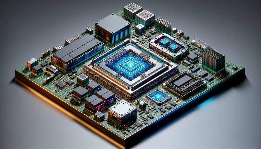
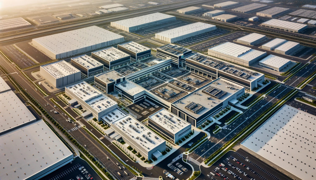
Premier On Semiconductor FAB And OSAT
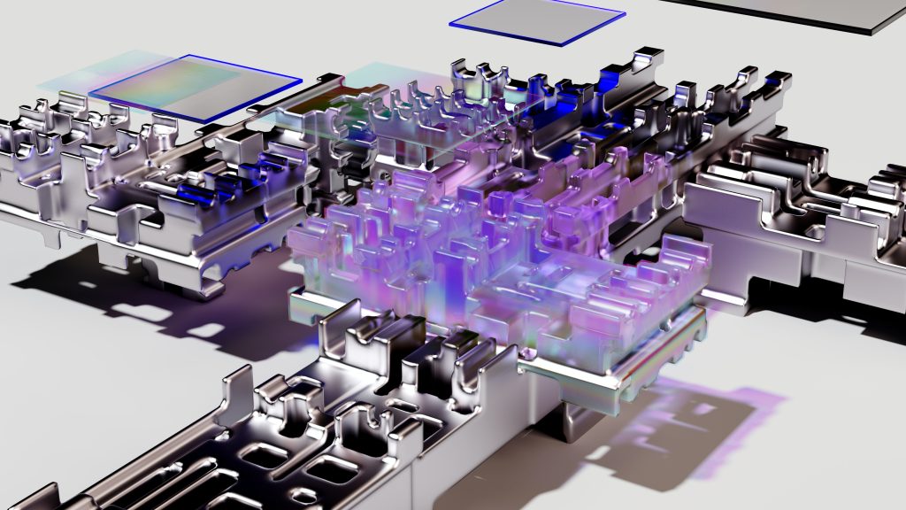
A semiconductor FAB is a production plant where devices such as integrated circuits are manufactured. These facilities are equipped with clean rooms and sophisticated equipment to precisely control environmental conditions, ensuring the high quality and purity required for semiconductor manufacturing.
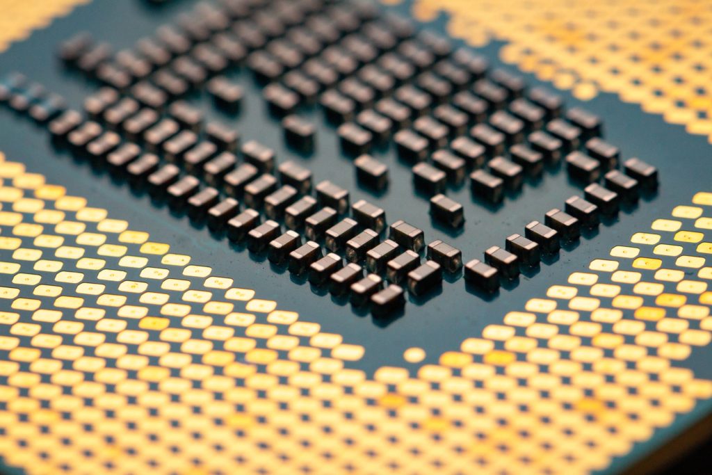
Outsourced Semiconductor Assembly and Test (OSAT) companies take over post-fabrication. They cut the manufactured wafers into individual chips, package them, and conduct rigorous testing (in many cases before cut/dicing) to ensure they meet the required specifications. OSATs allow semiconductor companies to focus on the highly specialized chip design process (and fabrication) without bearing the brunt of assembly and testing processes.
The Need To Invest In Semiconductor FAB And OSAT
Investing in semiconductor FABs and OSAT facilities is a strategic move for many countries and corporations aiming to bolster their technological infrastructure, economic resilience, and strategic autonomy.
As global demand for electronics continues to surge, the need for more integrated circuits rises, thus enhancing the strategic importance of having in-house semiconductor manufacturing and assembly capabilities.
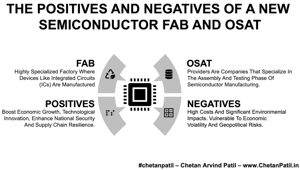
The Positives Of Semiconductor FABs And OSATs
Investing in semiconductor FABs and OSAT facilities is not just a financial decision but a strategic one that can significantly influence a nation’s or corporation’s technological and economic landscape.
The positives of such an investment revolve around enhancing economic activity through job creation and infrastructure development, boosting technological innovation, securing supply chains, and ensuring strategic independence. These benefits are crucial in positioning a country at the forefront of the global technological race.
| Aspect | Description |
|---|---|
| Economic Growth | Establishing FABs and OSATs involves significant capital expenditure, leading to job creation and infrastructure development, stimulating local economies. |
| Technological Leadership | Local FABs and OSATs foster innovation in semiconductor technologies, propelling advancements and maintaining a competitive edge in global markets. |
| Supply Chain Security | Having domestic FABs and OSATs reduces reliance on international suppliers, securing critical technology supply chains against global disruptions. |
| Strategic Independence | Domestic manufacturing of semiconductors ensures a steady supply of crucial components, vital for national security and technological sovereignty. |
Establishing FABs and OSATs can catalyze sustained economic growth and technological leadership. By fostering a self-sufficient and innovative environment, a country can significantly reduce its dependencies, enhance global competitiveness, and ensure a more secure future.
Moreover, the local development of semiconductor technologies can drive advancements in various high-tech sectors, cementing a country’s position as a technological leader.
The Negatives Of Semiconductor FABs And OSATs
Despite their significant advantages, establishing and operating semiconductor FABs and OSATs come with considerable challenges. The high costs of setup and maintenance, coupled with the environmental impact and the cyclic nature of the semiconductor market, pose potential risks.
Additionally, the geopolitical sensitivities associated with semiconductor supply can lead to vulnerabilities in international relations and trade.
| Aspect | Description |
|---|---|
| High Initial Costs | The cost of setting up and maintaining semiconductor manufacturing facilities can be prohibitively high, with risks of obsolescence due to rapid technological advances. |
| Environmental Impact | Semiconductor production is resource-intensive and generates significant hazardous waste, posing challenges for sustainable operations. |
| Economic Volatility | The semiconductor market is notoriously cyclical, which can lead to financial instability for regions heavily invested in these sectors. |
| Geopolitical Sensitivity | Being a critical component in numerous applications, semiconductor supply can be disrupted by international tensions and trade policies. |
While the negatives present formidable challenges, they necessitate robust planning and mitigation strategies to manage effectively. The high initial investments should be weighed against long-term economic returns, and environmental impacts require sustainable practices and technologies to operate.
Furthermore, navigating the cyclical economic patterns and geopolitical landscapes demands adaptive strategies that ensure stability and profitability in the volatile semiconductor market. These considerations are essential for countries and corporations aiming to capitalize on the benefits while minimizing the risks associated with semiconductor manufacturing.
What The Future Holds
The decision to establish new semiconductor FABs and OSAT facilities involves weighing significant positives against formidable negatives. At the same time, they promise economic growth, technological advancement, and many other benefits. Conversely, environmental impact, financial volatility, and geopolitical entanglements should also be considered.
As the global landscape evolves, the strategic calculation for investing in such infrastructure will continue to change, reflecting the dynamic nature of the semiconductor industry. Each country or corporation must carefully assess its capabilities and needs to make informed decisions that align with its long-term strategic goals.
By embracing innovation, prioritizing sustainability, enhancing supply chain resilience, and adapting to geopolitical and market dynamics, the semiconductor industry can expect robust growth and continued relevance in the global economy.
In conclusion, the future of semiconductor FABs and OSATs is promising but requires adaptation to a rapidly changing technological landscape and global context.