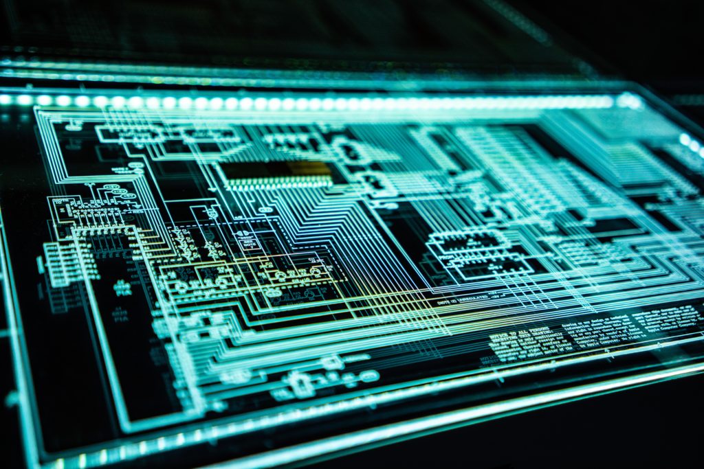
Photo by Adi Goldstein on Unsplash
THE NEED FOR WAFER VIRTUALIZATION
The use of virtualization techniques in the software and the hardware industry has enabled several technology developments. Virtualization provides developers the infrastructure to develop, test and deploy solutions catering both to the consumers and enterprises.
The three major types of virtualization occur at the application, operating system, and architecture levels:
Application: At the application level, virtualization provides a way to run an application inside a guest operating system that runs on top of a host operating system. It requires large memory and high-speed processors to ensure the memory level translation are fast enough to minimize latency when using the application inside a guest operating system.
Operating System: The operating system virtualization allows the developers to create containers to minimize (and almost eliminate) application dependencies when moving the application from one environment to another.
Architecture: The architecture level virtualization emulates guest instruction set architecture (ISA) on top of a host ISA, thus providing developers hardware features to test application behaviors on different architectures using one single target platform.
The above three virtualization techniques are post-silicon (majorly software) activities, which do not provide virtualization for silicon at the transistor level.
Wafer Virtualization Enables Pre-Silicon To Post-Silicon Die Level Semiconductor Design And Manufacturing Process Modelling And Simulation On Virtual Wafers.
Eventually, software/hardware virtualization will require a piece of silicon to run on. The development time and the cost involved to create the perfect semiconductor design and manufacturing recipes are way too high. To develop next-gen silicon-powered solutions also means a new approach to test and validate the technology-node and process (pre-silicon to the post-silicon) around it. On top of that, the silicon development technique should be affordable and drives faster development. The solution to the problem is wafer virtualization.
Wafer Virtualization: A virtualization technique that is driven by software modeling and simulation. It replicates pre-silicon to post-silicon activities at die level to create virtual wafers to validate end-to-end design and manufacturing process for the fast-paced technology-node development.
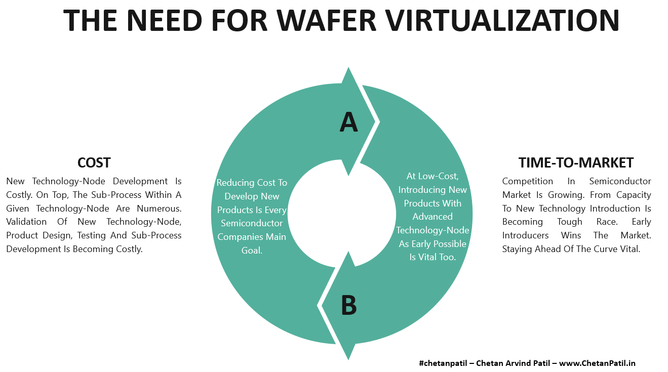
Wafer virtualization has numerous benefits. However, reducing cost and time-to-market are the two reasons for the semiconductor industry to invest more in the virtualized way of designing and manufacturing.
Cost: The cost of manufacturing using advanced technology-node is skyrocketing. The semiconductor companies often face challenges in opting for the next-gen technology-node and processes around it. No company wants to lose out on the benefits new technology-nodes have to offer. However, to fabricate samples for a new product using new technology-nodes, time and capital is required. While semiconductor manufacturing is a tightly controlled process, it often happens that there are device-level escapes that end up costing more when manufacturing proceeds without die/wafer level simulation. Process Design Kit is tightly controlled but does not offer a sneak peek at how the thousands of die on a wafer will behave.
Time-To-Market: The semiconductor market has stiff competition. The early launch advantage is the key. Semiconductor products utilizing the latest technology-nodes without prior validation often face challenges. More so, when the manufacturing flow requires masking to equipment level investment. Understanding the effect of a new technology-node or device/transistor changes on manufacturing is a time-consuming process. It is why a faster approach like wafer virtualization is required. It can help in capturing the effects of design changes on manufacturing. Eventually, it helps in reducing the time-to-market of new products.
The above two reasons make wafer virtualization a technique that should see large scale adoption. While there are already few companies that offer wafer virtualization, the solution is yet to get widely adopted for new product design utilizing new technology-node and devices/transistors.
Wafer virtualization will drive not only modeling and simulation of the design stages but will also enable virtual wafer fabrication. It can help with understanding how the process modulation (apart from electrical testing) impacts the design.
THE TWO SIDES OF WAFER VIRTUALIZATION
Wafer virtualization has the potential to reduce cost and time by enabling near-perfect data-driven design and manufacturing. It can provide insights to designers on how the circuit and internal components behave with the new technology-node or device/transistor changes. Wafer virtualization can also enable process level modulation that can drive iterative analysis of different design methodology.
However, wafer virtualization does have drawbacks while also providing several benefits:
Positive:
Early Look Ahead: Important advantage of wafer virtualization is the ability to provide early look data. This data can help in understanding the impact of the technology-node on design. It can also drive experiments to understand the effect of fabrication processes on the product design. Wafer virtualization can also help in understanding how the die and the full wafer behave to a different temperature to process modulation.
Multiple Iteration: Wafer virtualization provides numerous data analysis approach by tweaking devices or blocks within the product. The data gathered can provide insights on how the semiconductor product will behave due to minor/major process changes.
Low-Cost: The use of wafer virtualization guarantees that the capital and time invested, is utilized towards more cost-friendly analysis that can provide confidence to design and the manufacturing teams on product behavior. Companies can save time and thus can test/validate different products in the same given time.
New Methodology Testing: Designers often come up with novel approaches to design circuits. Wafer virtualization can allow innovative development to speed up the semiconductor product fabrication by quickly understanding the impact of design methodology on semiconductor fabrication.
Faster Iterative Process: Testing the same product with a different process is costly and time-consuming. Wafer virtualization enables the iterative approach to product development but from a die/wafer manufacturing point of view. Iteration on the design side is not easy. A middle path that strikes the balance of iterative design with manufacturing using wafer virtualization can aid the new way to design and develop.
Apart from above all the positive points about wafer virtualization, there are few negative/drawbacks of wafer virtualization.
Negative:
Validation Requires Silicon: Eventually, even after numerous unlimited number of simulation and modeling, the design needs to be fabricated into real silicon. Design is sent for fabrication only when the designers are satisfied with the data that wafer virtualization provides after all the variations and changes. It means a FAB and OSAT are eventually needed to bring the data into reality.
Modeling Errors: Wafer virtualization can go wrong if there are errors in the data due to incorrect analysis. Any type of modeling errors can be costly when the processes are locked and more so when the design files are already to FAB for fabrication. Another iteration will add to the cost.
Costly Data: Eventually, the data needs to get generated before it gets used for wafer virtualization. Some parts of the simulation leading to wafer virtualization can be via statistical methods. However, the transistor level functioning still requires validation with the real die/wafer-level data. It again requires investment in equipment and FABs that can provide the silicon sample data before the virtualization starts generating on its own.
FAB/OSAT Required: Wafer virtualization does not mean products being developed virtually for the customer use case. The final locked product will require FAB and OSAT to validate the virtualized wafer. Indeed, the gaps closed due to wafer virtualization can enable fewer errors than ever before.
Increase Development Cost: Investing in wafer virtualization also means added CapEx. For a FAB-LESS company, wafer virtualization can be key, but for an IDM it may mean added cost to the existing investment.
While there are both positive and negative aspects of wafer virtualization, in the long run, the benefits of wafer virtualization due to data provided that is very close to the manufacturing process is vital.

THE IMPACT OF WAFER VIRTUALIZATION
Given the numerous use cases of wafer virtualization in the end-to-end semiconductor design and manufacturing process, the impact it can have on semiconductor device development can push the boundaries of next-gen device/transistor design.
The impact of wafer virtualization use can be seen both on academia and the industry:
Academia: Researchers can implement modeling and simulation for wafer virtualization to drive the development of die/wafer-level solutions. It can provide data on how the design changes at the device/transistor level can impact the post-silicon process. Researchers can develop a new device/transistor design and see how it performs across different technology-node. The promising solutions can then be used by industry to enable next-gen semiconductor products.
Industry: Apart from balancing cost and time-to-market, wafer virtualization can drive internal research and development activities are geared towards the market a few years down the line. The semiconductor companies can benefit immensely by leveraging data that ensure robust More-Than-Moore solutions.
Wafer virtualization is a promising solution for an industry that requires products to meet strict standards. The requirements to meet from pre-silicon to post-silicon stage are vital too. With the face-paced technology-node development, wafer virtualization can provide a new way to design and manufacture semiconductor products.


