Photo by Florian Olivo on Unsplash
THE MAJOR BLOCKS OF THE SEMICONDUCTOR FOUNDRY ROADMAP RACE
Semiconductor foundries across the globe are focused on providing solutions to retain existing customers and attract new customers. To achieve these two goals, semiconductor foundry companies have to keep innovating. Innovations are critical to ensure the solutions offered by foundries will spearhead the growth of new semiconductor products, thus the customers.
Semiconductor foundry roadmap plays a vital role in empowering customers with the future of semiconductor foundry technology. These roadmaps require years of research and development and are often in line with where the semiconductor industry is heading. Roadmaps also attract investors, and achieving roadmap milestones without delay is more important than ever. Any slip in achieving the milestones can directly impact customers and can derail market position.
The semiconductor foundries focus on several aspects of semiconductor technologies to drive semiconductor manufacturing forward. However, there are specific blocks that the majority of the semiconductor manufacturing players focus on as part of their long-term roadmap.
Technologies: Semiconductor foundries run on different types of semiconductor technologies. These semiconductor technologies are driven based on the product focus and capabilities of a given foundry. Semiconductor foundry fabricating only memory devices is more inclined towards (Example: Micron focuses on novel ways to increase layers of memory cells) providing memory-oriented semiconductor technologies. Similarly, analog, digital, or mixed-signal fabricating foundries focus on next-gen photo masking, etching, passivation, lithography, etc., to set their fabrication technology apart. The drive to focus on a specific technology (as per the foundry requirement) is the primary reason the yearly semiconductor roadmaps (from different companies) are focused on solutions that can enable future semiconductor technologies (devices, materials, etc.). Doing so can also expand the market share.
Devices: Devices are the basic building block of any silicon product. In the last few decades, the size of these devices (FETs) has only shrunk, thus providing more area to pack different types of processing blocks without utilizing a large silicon area. These devices have shrunk in size due to the massive research and development (between academia and industry) activities coupled with advancements in semiconductor equipment technology. Device research and development activities also need to be part of roadmaps to ensure next-gen solutions (like MBCFET, Next-Gen FinFET, etc.) cater to the requirements of both the foundries and the design houses.
End-Of-Line: Semiconductor fabrication requires three different lines/steps: Front, Middle, and Back. Front-End-Of-Line (FEOL) focuses on creating the structures that make the chip active as per the voltage and current requirements. Back-End-Of-Line (BEOL) process steps are primarily concerned with connecting different layers/blocks via complex interconnects. Lastly, to bridge the gap between the FEOL and BEOL, Middle-End-Of-Line (MEOL) is required. MEOL provides structures that serve as small contacts (like interconnects but have a specific and niche use/purpose during the fabrication) between different active regions of transistors. These three fabrication steps are the base of any silicon product. To keep up with Moore’s law, FEOL, MEOL, and BEOL have to be on the semiconductor foundry roadmaps so that every foundry can differentiate its process technologies from others and in the long term can provide unique solutions.
Materials: Similar to semiconductor devices, semiconductor materials also are one of the building blocks of semiconductor products. In reality, semiconductor products heavily utilize semiconductor materials during the manufacturing steps. The semiconductor foundry business will not exist without semiconductor materials like Silicon, Germanium, Gallium Arsenide, and several more. Apart from the basic periodic table materials, the semiconductor industry is also dependent on different kinds of chemicals. In the end, the semiconductor industry is built on top of basic science like any other industry is. Almost all semiconductor foundries focus on the materials aspect. However, given the slow change in new techniques around materials, the emphasis on semiconductor materials is not as big as any other aspect of semiconductor fabrication. Continuously improving the device efficiency means that the semiconductor foundries also need to focus on new types (Carbon nanotube, compound semiconductors, etc.) of materials to enable new solutions.
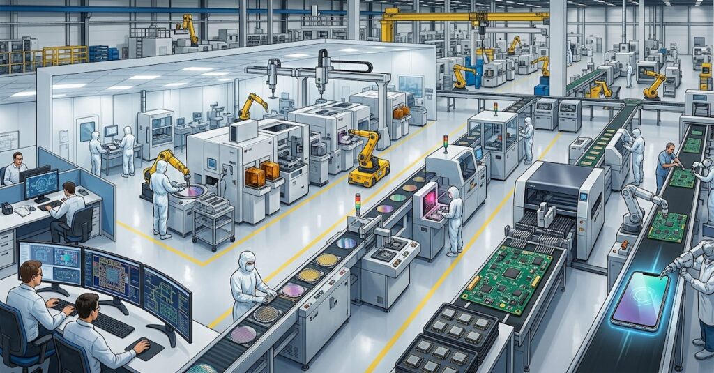
Automation: Semiconductor manufacturing (fabrication, assembly, and testing) is highly automated and requires minimal human interference to process the wafers. Semiconductor automation plays a vital role in ensuring that the lots get processed with the maximum throughput possible. Along the way, automation also captures/predicts issues that can empower semiconductor foundries with information to avoid delays and cost. The importance of automation has only grown in the semiconductor industry, and the dependency means automation technologies have become the default part of the semiconductor foundry roadmap.
Semiconductor foundries have focused on roadmaps for decades. It has helped them come up with next-gen technology and has also pushed the semiconductor technology race forward. Semiconductor Pure-Play Foundries and Integrated Device Manufacturers (IDM) are known for charting specific roadmaps that have always driven semiconductor manufacturing forward.
However, as the race to come up with the next-gen semiconductor manufacturing solutions grows, there is a need to focus on specific solutions that can push the manufacturing aspect of the semiconductor towards the angstrom era of devices.

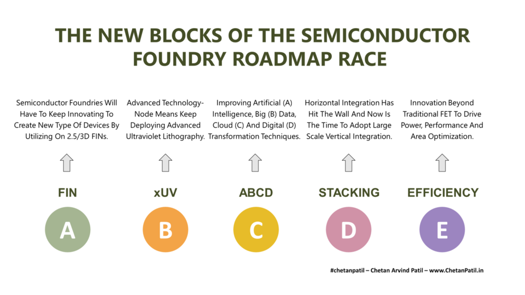
THE NEW BLOCKS OF THE SEMICONDUCTOR FOUNDRY ROADMAP RACE
The continuous integration of new devices without increasing the silicon area has provided a new path for semiconductor design and manufacturing. Today, slim and compact electronics products are only possible due to the advent of a new class of semiconductor devices and technology-node that have ensured that the area required is not a hindrance to providing required power and performance.
Semiconductor researchers in collaboration with foundries have focused on several semiconductor technologies that have pushed the boundaries of semiconductor manufacturing so far. In the years to come, semiconductor foundries will need to focus on the new (examples below) building blocks of a roadmap for the semiconductor foundry.
FIN: The building blocks of semiconductor products are the devices. Until FinFET, these devices were planar. Starting with FinFET, the semiconductor design moved towards 2.5D. However, the need to scale further and put more transistors without compromising power and performance requires using 3D devices built using nanowire (GAAFET) and nanosheets (MBCFET). For increasing transistor density beyond Moore’s era, the semiconductor foundries will have to look into future devices that can utilize the FINs on the FET to drive the industry beyond 1nm and into the Angstrom era. It will require different foundries to focus heavily on a roadmap that purely focuses on developing new multi FIN-based FET devices.
xUV: Lithography is one of the critical fabrication process steps and also the costliest of all. Today, the most sophisticated UV technology to drive lithography is Extreme Ultraviolet (EUV). Only a handful of semiconductor foundries around the globe are capable of fabricating wafers using EUV equipment. The reason is the cost and also the fundamental issue like defects leading to reliability concerns. Technology like EUV is critical to meet semiconductor foundry’s technology-node goals. The semiconductor industry is on its way to surpass 2nm technology-node, which will require cost-effective and error-free lithography techniques that can enable devices transistors size of 1nm and beyond. It is only possible if semiconductor foundries work with semiconductor equipment manufacturers to drive a roadmap for next-gen lithography technology-powered equipment.
ABCD: Semiconductor foundries are fabricating hardware devices, but doing so requires several software solutions to keep the production line up and running apart from achieving the high yield, low defect, and faster throughput. All this is possible due to the focus on the ABCD (A = Artificial Intelligence, B = Big Data, C = Cloud, D = Digital Transformation) approach the semiconductor foundries have taken for a long time. As the world moves towards new semiconductor capacity, the need to drive next-gen ABCD solutions that are low on cost but high on efficiency will grow. Semiconductor foundries will have to keep innovating internally to ensure that the ABCD approach gets implemented via a roadmap to achieve the target (yield, scrapping, errors, etc.) results to drive minimal waste with maximum output.
Stacking: FinFETs tool the semiconductor industry from 2D devices to 2.5D devices. And today, the semiconductor industry is gearing to expand the FINs to enable the next-gen devices like CFET. CFET utilizes the folding approach to keep nFET on top of the pFET, thus securing the stacking approach for a real 3D integration. Stacking will also ensure that the next-gen devices utilize far less silicon area than today’s devices. It also requires innovation on the package-technology side, but the first step is always fabrication. Several device-level solutions exist that can transform horizontal integration into vertical. It will ensure the semiconductor industry keeps increasing the transistor density. However, there are still thermal, electrical, and failure (apart from cost) challenges that require a continuous improvement plan with the help of long term stacking roadmap.
Efficiency: Semiconductor products are defined based on how efficient they are. Efficiency does not mean low-power consumption but is about achieving the perfect balance of power, performance, and area (PPA) as per the target application. To achieve the balance of PPA, several semiconductor technological solutions from equipment, wafer size, devices, materials have to come together. Devices might be the most dominating aspect of achieving a balanced PPA. However, to fabricate these devices, different other semiconductor building blocks are required. Semiconductor foundries will have to have a roadmap that focuses on the power, performance, voltage, and area characteristics of the next-gen technology-node is at par with any given solution that exists today.
Several semiconductor manufacturing companies are gearing up to increase the worldwide installed semiconductor manufacturing capacity. However, increasing capacity is only half the job done. What is needed is the focus to keeps bringing new semiconductor manufacturing technologies that can excite the customer and drive the market towards a new era of semiconductor solutions.
The new upcoming semiconductor foundry capacity will require a semiconductor roadmap that drives new types of technology-node, equipment, automation, and other solutions. Semiconductor foundry’s roadmap from different competitors will ensure tomorrow’s semiconductor products are better than today’s and will also push the innovation around the products that semiconductor silicon devices are powering today and in the future.
