
Photo by Brecht Corbeel on Unsplash
Generative AI (GenAI) is creating new ideas and the market for the software industry. Software developers are using GenAI to develop tools to revolutionize the digital world. Per experts, we are only getting started with GenAI. And, at some point, the semiconductor industry will have to adapt to the GenAI way of working.
Examples of how GenAI can help with semiconductor design and manufacturing:
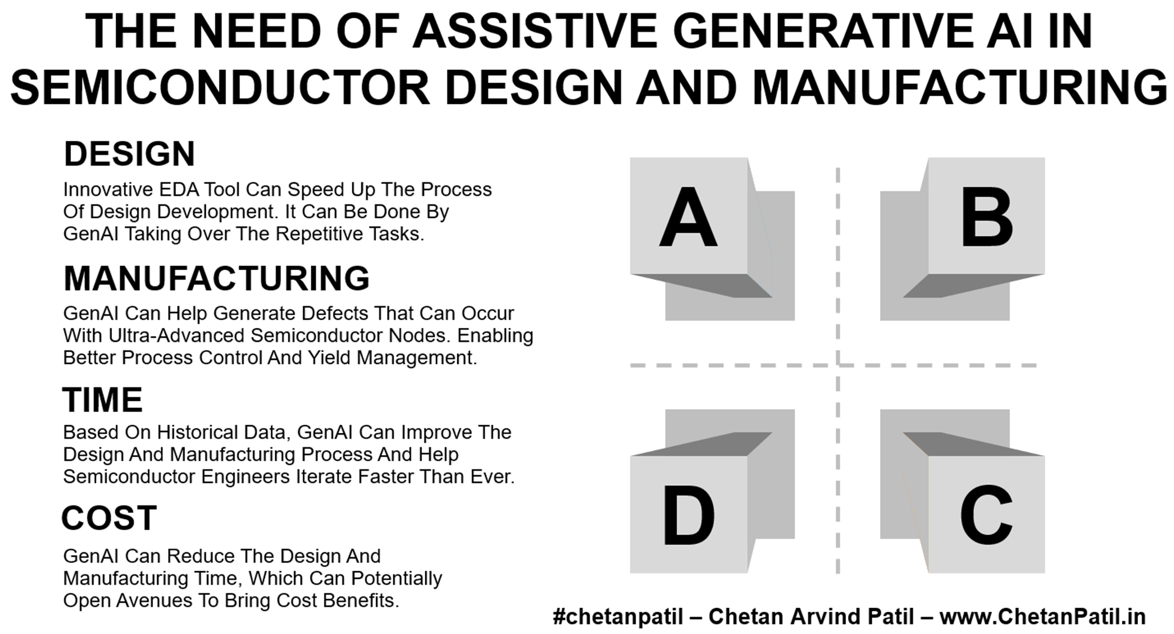
Design: Smarter EDA tool can speed up the process of design development. It can be done by GenAI taking over the repetitive tasks. GenAI can also capture errors on the go and suggest better design optimization techniques. And slowly, based on the historical data, help designers build optimized solutions.
Simulation: Simulating the design and capturing the data to validate the specification is critical to the semiconductor design process. As the complexity of the circuit design increases, the GenAI-based simulation tools can help the designer by providing better-summarized data, swiftly comparing it with similar past design databases to reveal critical insights and, in turn, can also develop new models to predict different reliability to characterization profiles accurately.
Defect Generation: Process control and yield management are critical to achieving the highest ROI in any semiconductor manufacturing environment. GenAI can help generate defects that can occur with ultra-advanced semiconductor nodes. This information can enable faster and more accurate classification of yield issues and capture issues on the go.
Planning: As much as semiconductor design and manufacturing is about technical understanding, a lot also depends on the planning aspect. Aside from resources, scheduling, and development, it is vital to product launch. GenAI can be a game changer by creating better flows of executing and planning by considering different data points from past learnings and failures.
While GenAI itself will not be able to take over 100% of the design and manufacturing process of semiconductor products, on the other hand, it can act as a catalyst to help drive assistive design and manufacturing.
It is precisely the type of solution the semiconductor industry needs so that the advanced semiconductor technologies around Moore’s law and More Than Moore drive new design and manufacturing methods forward faster.
The impact of slowly deploying semiconductor-focused GenAI solutions will have a positive effect on the way the design and manufacturing of semiconductors occurs.
The significant benefits of utilizing the GenAI capabilities are as follows:
Time: Assist in the silicon block design and provide a better view of further optimizing for performance, power, and area. The assistance by GenAI, based on historical data, can improve the design and manufacturing process and help semiconductor engineers iterate faster than ever.
Corrections: Finding bugs in the design and manufacturing flows and presenting them ahead of time is also something GenAI can help the semiconductor industry with. It can significantly reduce costs and drive companies towards defect-free products.
Efficiency: One of the fundamental goals of any new silicon chip or process node is to improve performance and manage power/energy consumption. To build better efficient designs and processes, reviewing historical data is critical. And this is where GenAI can bring a gaming-changing solution and assist design/manufacturing teams in speeding up the process.
Cost: If the solutions around GenAI can reduce the design/manufacturing time, bring zero defect products and reduce the silicon ideation to validation to sampling to production time, then the potential cost benefits are many.
Confidentiality is one of the biggest hurdles in deploying GenAI solutions in the semiconductor industry. To some extent is a valid concern, as the semiconductor companies will never know how deploying GenAI solutions can lead to critical information leakage, which can be catastrophic.
To tackle this, semiconductor design and manufacturing companies must develop a process allowing them to build GenAI-specific tools in-house or, at the least, trust the vendors they are working with to provide a tailored solution that ensures the sandbox created is complete and leakproof.
Eventually, the semiconductor industry has to catch up with the software industry on the GenAI front. Otherwise, the development speed in the software domain will be 100x, and the semiconductor industry will follow the 10x speed, creating new age bottlenecks for both sectors.


