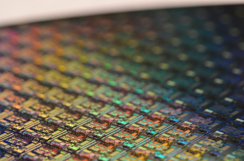
Photo by Laura Ockel on Unsplash
THE END-TO-END SEMICONDUCTOR CLUSTER ECOSYSTEM
The semiconductor industry is vital for high-tech advancement. From smartphones to satellites, a small piece of silicon forms the base for millions to trillions of data points. It is why worldwide, the semiconductor industry is a Key Enabling Technology (KET) provider. Semiconductor product development requires various resources to come together. With the growing demand for smart hardware, the need to develop these resources in-house is more critical than ever.
In semiconductors, no single country wants to be 100% reliant. Countries are ramping up in-country semiconductor design and manufacturing efforts.
The complexity of both the design and the manufacturing aspects of semiconductors makes it a tough business. It takes years and decades to come up with a turnkey ecosystem to drive in-country semiconductor design and manufacturing. The cutting-edge technology that is required to become self-reliant in semiconductor design and manufacturing demands a radically different approach than incentive-based schemes, which the majority of the governments provide.
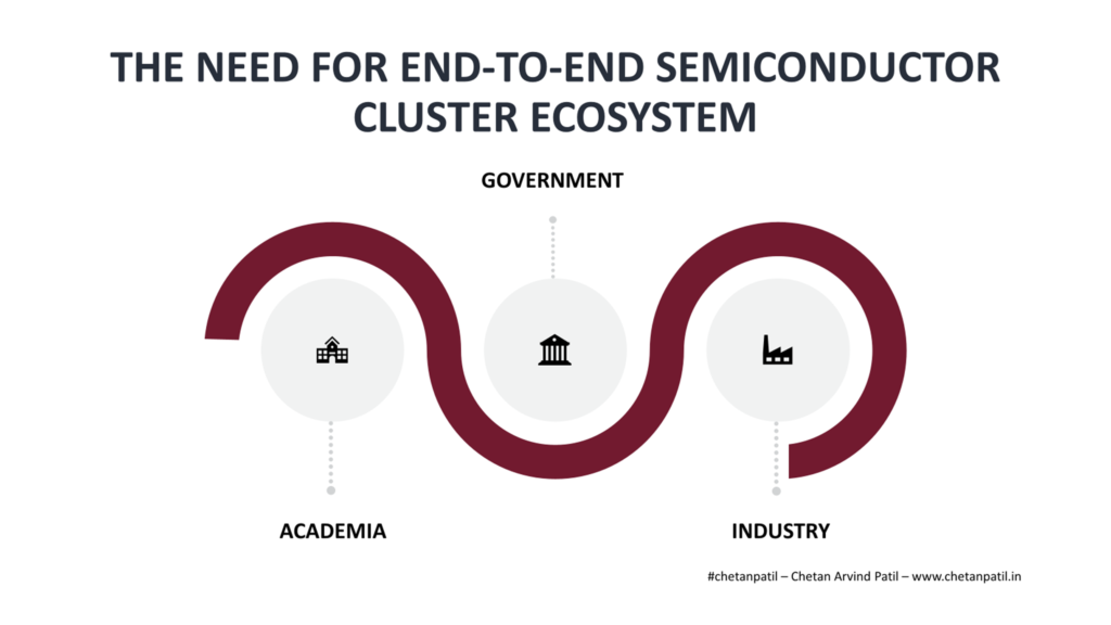
The End-To-End Semiconductor Cluster Ecosystem Requires In-Country Development And Growth Of Semiconductor To Drive Key Enabling Technology
End-To-End Semiconductor Cluster Ecosystem: An end-to-end semiconductor design, manufacturing, and support ecosystem that enables seamless semiconductor product development. It requires different components of the semiconductor product development to be done in-country rather than globally. It drives in-country economic and talent development and is cost and time effective.
The End-To-End Semiconductor Cluster Ecosystem is what countries should focus on building to pitch themselves as a one-stop destination for all semiconductor solutions. However, it is easier said than done. The list of different types of resources and solutions that are required to develop a semiconductor cluster ecosystem is long. Depending upon the market size and focus area, countries can have a different smaller focused end-to-end semiconductor cluster ecosystem that has all the components of semiconductor design to manufacturing to customer delivery.
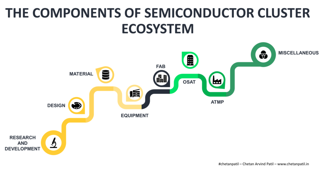
THE COMPONENTS OF THE END-TO-END SEMICONDUCTOR CLUSTER ECOSYSTEM
Creating a semiconductor cluster ecosystem is not easy. There are different components required to ensure that the environment supports the semiconductor business. Following are the major components of the semiconductor cluster ecosystem:
RESEARCH AND DEVELOPMENT
Research and Development (R&D) is key to both basic and applied science innovation. R&D requires the cooperation of government, academia, and industry. Given how complex semiconductor product development is (from technology node to packaging to power requirements), continuous and steady R&D spending is vital as it forms the base of the semiconductor cluster ecosystem.
According to the Semiconductor Industry Association, in 2019, the U.S. semiconductor industry R&D spending was 16.40% of total sales. Europe spending was 15.30% of total sales, while Taiwan, Japan, China, Korea spending was 10.30%, 8.40%, 8.30%, 7.70%, respectively. It clearly shows the importance of R&D spending and how it helps drive the leadership in the semiconductor business.
Countries wanting to implement the semiconductor cluster ecosystem need to increase R&D spending by collaborating with academia and industry, to drive advanced solutions for the market.
DESIGN (FAB-LESS/EDA/IDM):
Without the semiconductor design, there is no manufacturing. Countries around the globe are attracting businesses to design in-country. This requires setting up of FAB-LESS business which can drive the design of Analog, Digital, Processor, Memory, and Sensor-based products. To cater to the needs of FAB-LESS, EDA companies are required who can provide software-based tools to drive circuit to layout design, simulation, and validation. Apart from FAB-LESS, there are several IDMs (Intel, NXP, Marvell, etc.) which cater to the need of both the design and manufacturing aspect of the semiconductor.
The development of an in-country design ecosystem requires a talent pool. This demands universities with excellent infrastructure that can provide deep technical training required to drive gain expertise in semiconductor engineering.
MATERIAL:
No FAB or OSAT in the world produces the materials required to bring the silicon to life. Different chemicals, silicon, photomasks, gases, substrates, compounds, etc., are required to develop the wafers and packaged materials. There is a big dependency on specific countries and companies that provide such materials.
Semiconductor material development and procurements also mean a good understanding of the engineering aspect and as said it requires heavy R&D activities within the country where the materials eventually will get used, either by the FAB or the OSAT.
EQUIPMENT:
Semiconductor equipment is a billion-dollar market. Both FAB and OSAT require heavy machinery to process and assembly wafer silicon. ASML is the largest supplier in the world of lithography systems for the semiconductor industry apart from ASM, Applied Materials, and TEL. On the other hand, ADVANTEST, TEL, and Teradyne are the largest supplier of ATE-related equipment.
Both FAB and OSAT equipment are vital to ensure the materials and design eventually get made in the form of a product. A country with a stronghold on the semiconductor equipment manufacturing market is key to anything semiconductors.
FAB:
Fabrication of semiconductor devices requires dedicated facilities with large clean rooms. The investment to create such a facility is big and is the primary reason why there is only a handful of semiconductor FAB around the world. Even out of the existing FABs, not all are equipped to handle the advanced technology node that the semiconductor industry has ventured into.
TSMC, Intel, GLOBALFOUNDRIES, and Samsung Semiconductor are competing with each other to grab the opportunities presented by technology node 5nm and beyond. To make countries self-reliant in semiconductor, FAB play a vital role. It has pushed governments without any FAB facilities to provide incentives to set up new advanced FAB. However, setting up FAB also requires a supporting ecosystem, and this is why countries should focus on the cluster-based ecosystem that provides in-country end-to-end semiconductor solutions.
OSAT:
Outsourced Semiconductor Assembly And Test (OSAT) is as important as FAB. Packaging the products with the right technology enables long life. Testing every die on the wafer is vital to ensure there is no reliability or test escape. OSAT enables defect-free parts to the customer. They drive the back end of semiconductors, which in itself is a billion-dollar market.
Historically, OSATs have been located in the Asia Pacific and have been dependent on America and Europe due to the R&D and design lead these two continents hold. For a semiconductor cluster ecosystem, all the major components need to be catered to, not only specific ones. This is why OSAT is trying to get into FAB and is also investing in in-house design.
ATMP:
Assembly, Testing, Marking, and Packing (ATMP) is different than OSAT. OSATs take the bare wafer silicon and convert it into a packaged product, which is then shipped to the ATMP houses. ATMP receive packaged semiconductor products from different OSATs and then they assemble it together on a printed circuit board (PCB). All the semiconductor devices are connected to form a working computer system and clear marking details are put on the PCB to ensure traceability of devices. As the last step, the PCB is covered with an aluminum or plastic body before being shipped to the customer in a fancy box.
China is the leader in ATMP. India is another upcoming destination. Dell and Foxconn are the world’s largest ATMP houses. Having ATMP houses in-country provides economic development but at the same time negates the benefits when a country becomes 100% importer of semiconductor products. This is what has happened with India’s ATMP ecosystem.
MISCELLANEOUS:
Apart from all the major components, there are some crucial minor components that are also critical for the semiconductor cluster ecosystem. These include logistics, distribution, and enterprise-level software. Having delivery and development houses for these activities is also critical in ensuring an end-to-end semiconductor cluster ecosystem. Given these solutions are driven mostly by software in today’s day and age, the majority of countries have both development and R&D centers catering to the future of how to efficiently to logistics to distribution with the help of data and software.
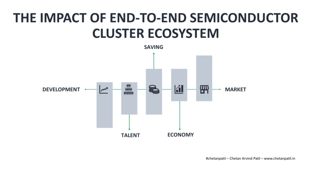
SUMMARY: End-to-end semiconductor cluster ecosystem requires all of the above components to be in close proximity. However, as of today, there is not a single full end-to-end semiconductor cluster ecosystem in the world. The majority of the semiconductor cluster ecosystem has one or max three of the above components. Given the race between countries to attract the world’s best semiconductor business and talent, the focus on the end-to-end semiconductor cluster ecosystem needs to increase by leveraging facilities within the same location or country. Having more FABs and then relying on other countries for OSATs and ATMPs is never going make a single country the destination for all semiconductor needs, and that is what the majority of the countries in the last two to three years are trying to achieve. Unfortunately, that is not possible till an end-to-end semiconductor cluster ecosystem is built in-country.
THE ACTIVE SEMICONDUCTOR CLUSTER ECOSYSTEM
There are a handful of semiconductor cluster ecosystems located in different countries. However, these clusters do not cater to all the components discussed above. It will not be valid to call these centers a semiconductor cluster ecosystem, but it does show the importance of having one or more semiconductor components within vicinity.
Following are a few active semi semiconductor cluster ecosystem but not end-to-end:
Intel – Portland, Oregon, USA And Chandler, Arizona, USA: Intel has advanced FABs in Portland, Oregon, and Chandler, Arizona. There are two big universities in the proximity of these two FAB locations: Portland State University and Arizona State University. Cross-industry and academia collaboration at these two locations have to lead to the launch of several innovative semiconductor solutions. The exchange of talent for research activities has also helped. Intel’s presence in these two locations guided the formation of a semiconductor support environment that has helped its FAB execution. This is also the primary reason why TSMC has chosen Arizona as the destination of their next 5nm plant.
ASE Global – Kaohsiung, Taiwan: ASE Global has multiple OSAT facilities in Taiwan. Kaohsiung plant stands out due to the proximity to other package technology solution providers like Amkor. The competition has helped with the development and availability of the semiconductor raw materials required to smoothly operate an OSAT facility.
TSMC – Hsinchu, Taiwan: TSMC has several FABs around the globe with the majority of the FABs located in Hsinchu, and has helped TSMC develop an ecosystem that has allowed universities and OSAT nearby to thrive. Having OSAT and FAB in the same location also reduces the cost and time of product development.
Newport Wafer Fab – Newport, United Kingdom: Newport Wafer Fab is the latest addition to the semiconductor ecosystem and promises to be the one-stop FAB needs for the UK region. It has tied up with Cardiff University to enable future compound semiconductor development. Showcasing why having universities nearby helps.
Samsung – Gyeonggi, China: Samsung like TSMC has FABs in a different part of the world, with the majority located in Gyeonggi. China being home to both the OSAT and ATMP houses, has allowed Samsung to take advantage of the in-country ecosystem of semiconductors.
TAKE AWAY: Above examples show the importance of having one or more semiconductor cluster ecosystem components in proximity. Imagine having all the semiconductor components in one location and that too within a single country. The benefits from employment, development, and growth will be immense. Whether or not such an ecosystem will end up getting developed, but for sure, countries are racing to attract the best talent and semiconductor businesses to drive in-country semiconductor growth.
THE WAY FORWARD FOR END-TO-END SEMICONDUCTOR CLUSTER ECOSYSTEM
The semiconductor industry is going through massive critical changes. From mergers to acquisitions to new companies to new FABs, all this is shaking up the semiconductor business.
Traditionally, semiconductor design and manufacturing has been all about specific regions/countries in the world having a stronghold on either the design or manufacturing or equipment. Post-2020, the story is going to change. Majority of the country has already started chasing giants of the semiconductor industry to set up their designs for manufacturing houses.
Country With The End-To-End Semiconductor Cluster Ecosystem Will Lead In The Digital Technology World.
Governments need to develop their country as an end-to-end semiconductor cluster ecosystem, with a solution for every component of the semiconductor development cycle. Having one facility and not the other is only going to make the new facilities in the new country dependent on the old facilities in other countries.
The country that can create an end-to-end semiconductor cluster ecosystem is going to have an advantage over others and will lead the digital technology competition.


