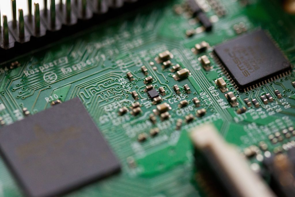
Photo by Chris Ried on Unsplash
The shrinking size of semiconductor nodes has led to better performance, which is beneficial from a features point of view, but not from the cost point of view. The cost to design and manufacture highly complex chips (to provide better performance) is increasing year on year. It is thus pushing the semiconductor industry towards solutions that enable new features but are also not high (long term) on cost.
To balance the cost with features, semiconductor researchers (academia and industry) have focused on solutions that are not high on investment and at the same time provide a way towards the More-Then-Moore era.
The one approach that researchers have taken is to focus on the silicon devices and then invent improved versions that provide balanced (power, performance, thermal, and voltage) characteristics. One example is photonic devices, which enable high-speed communication and are getting adopted for advanced silicon chips.
Neuromorphic Devices: Lately, neuromorphic chips have been the focus of the computing industry. It has given rise to the IP that enables pre-configured devices with more adaptive features than ever before. Such devices are suitable for real-time applications where algorithms demand faster computation.
Flexible Devices: Flexible electronics is another approach that the semiconductor industry is adopting. The flexible devices present an opportunity to stack silicon (mainly packages) uniquely. So far, flexible devices are limited to the board-level solution and follow a hybrid approach. However, soon unique material properties will drive flexibility architecture level.
There has been an increase in the adoption of devices that scale vertically instead of horizontally. However, in the long term, such a solution will hit the node wall, and thus the semiconductor industry will have to adopt a non-scaling approach.
To tackle such scenarios, devices like neuromorphic and flexible present an excellent opportunity as these devices can enable advanced adaptive features coupled with the flexibility to adopt different form factors, which can benefit different types of computing silicon chips and solutions.
There are several known reasons why the scaling approach is not going to work beyond a certain point, and the two most critical reasons are the cost and device operating budget. The cost factor is associated with the manufacturing aspect of the semiconductor, while the device operating budget is all about creating technical criteria that fit the performance and power requirements of the given application/solutions.
Even the most advanced devices will hit the node wall where scaling will not be a cost-effective feature. The efforts and investment required to bring next-gen (FET-inspired) devices may not provide long-term sustainable solutions. Hence, the semiconductor industry needs to mass-produce complementary solutions that are scaling avert and can co-exist along with the standard devices.
Carbon Devices: Carbon Nanotube FETs (CNFETs) have been in the works for a very long time. After decades of research and development, the industry has started adopting CNFETs. However, they still suffer from a power handling and have yet to be mass manufactured.
Photonics Devices: Photonics is vital for optical communication and also for interconnects. There are already several companies that have provided a way forward for the mass adoption of photonic devices, and several new silicon-powered devices are already showcasing the potential of photonic-based solutions.
Investment and the resources required to enable emerging devices are very high. It is why public bodies and governments will have to provide the much-needed runway for academia and industry. It will ensure the long-term foundation for the research and development of the futuristic device.
The next decade is going to bring new emerging devices that will not only provide advanced features but will also drive the semiconductor industry towards a new era. The vital part will be to enable faster adoption and manufacturing.


