
Photo by Jorge Salvador on Unsplash
THE COSTLY LIFE CYCLE OF SEMICONDUCTOR DATA
The importance of data in different industries has only grown over the last few decades. This has in turn given rise to different new techniques and tools that enable enterprises to capture and analyze data on the go. It will not be wrong to say that today, the most prized commodity in the market is data.
The same story is applicable in the semiconductor industry. The shrinking transistor size and the need to enable efficient devices has increased the importance of capturing data from all the possible semiconductor product development process. However, the major hurdle in doing so is the cost associated with the process.
Semiconductor Data Is The Next-Gen Oil.
Shrinking transistors enable better devices and empower the long-term product development roadmap. Though, when it comes to the cost part of it, things start to get complicated. Cost is also the major reason why there are only three players (Intel, Samsung, and TSMC) that are battling the 5/3 nm race. The cost required to set up the FAB and the support system (equipment, facilities, tools, resources, and many other things) is too high and often requires long-term investment-wise planning. Even building a MINI-FAB today, will require billions of dollars to set up, and there on will take years to break even.
Setting up smaller research and development facility is an efficient way to capture semiconductor data, but it is not feasible to rely on smaller labs/setups for too long. In order to meet the worldwide demand, the facilities eventually have to expand.
– MINI-FAB >$1 Billion
– MEGA-FAB > $4 Billion
– GIGA-FAB > $12 Billion
– MINI/MEGA/GIGA = Defined Based On Wafer Capacity.
This makes the process of capturing and handling the semiconductor data crucial. Any data point that comes out of the pre-silicon or post-silicon stage has to go through a specific life cycle before being stored for long-term usage. This life cycle data handling process itself adds additional cost apart from the FAB investment. In the long run, the semiconductor companies understand the importance of setting up the data life cycle flow and have always invested relentlessly both in the process that leads to silicon and also the process required to generate data out of different silicon products.
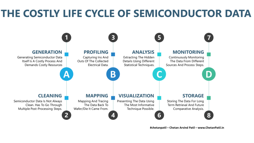
Below is an overview of how the semiconductor data is handled and why each of these processes is vital. In nutshell, these steps are no different than how any big data will get handled. When it comes to the semiconductor industry, the major difference is the effort (cost and resources) it takes to generate data from different types of semiconductor products that often require large setups.
Generation: Generating semiconductor data requires a silicon wafer (with dies that are testable) and a test program that can run on the full wafer. Both of these processes demand different sets of tools and resources. A dedicated FAB is tasked up with creating a silicon wafer that has the product printed (repeatedly) across the full area. Which in itself is a costly process. On the other hand, a dedicated tester environment (OSAT) with different hardware and equipment is required to drive the test program. Such a long and delicate process not just requires product but also manufacturing, logistics, handling, and equipment resource. The sum of all these investments eventually allows semiconductor data to be generated. And without going into details, is understood how costly and time-demanding process this is.
Cleaning: Generating data out of the silicon is the first step. As explained above, it requires different sets of hardware equipment to drive the semiconductor data generation. The data in the majority of the cases are generated in a standard format, but still require a lot of post-processing and elimination techniques to make sense of it. This cleaning process is more on the software side and demands data processing tools that can help engineers understand different features of the silicon data. The cost associated is due to the setting up of the flow that allows semiconductor companies to capture the data at the source, which can then be easily sent to the servers for engineers to retrieve. There on, the cleaning steps start.
Profiling: Simply collecting random silicon data is not useful. The semiconductor product itself is going to be used in different systems and environments. This environment will push the product through different operating conditions. To ensure the product works under different conditions (temperature, process variation, current, and voltage settings), the development phase pushes the product/silicon through several testing criteria. These are often based on the industry-accepted standards (AEC, JEDEC, IPC, etc.). Carrying out all these tests to gather the promising semiconductor data (that will qualify the semiconductor product for the market) is challenging. The cost associated with it is also on the rise and thus adds another costly layer towards capturing the semiconductor data.
Mapping: The semiconductor data is often captured in big chucks. This can be at the wafer level or lot level. In both cases, it becomes really important to ensure that the data can be traced back to the die/part it originated from. The process to do so starts much before the test data is available. This can be via different marking to memory-based traceability techniques. This again points to the fact that the data mapping also requires base resources to achieve the target of not only ensuring the semiconductor data is available, but it is also easy to map it back to the source.
Analysis: Post all the possible data is captured and is available for engineers, the main task starts. While clean data (no skews or deviations) is the dream of every engineer, however, even with the cleanest data it becomes crucial to question different aspects of it. And, if there is a fail part, then finding the root cause is a must. This process requires sophisticated data exploration tools that bring efficiency. These tools should also be able to connect back to any historical/relevant data that can answer any deviation or miss alignment with new data. If data cannot answer all the questions, then comes the interesting part of putting together the root cause analysis plan. All this is not only a time-consuming process but also demands costly resources.
Visualization: Analysis and visualization go hand in hand. However, not all the tools are great at both the analysis and the visualization part. This pushes semiconductor data engineers towards exploring the data using different tools. In the majority of the cases, these tools are procured from the software data industry. But it also happens that the companies are willing to invest internally to come out with an easy visualization technique that can provide information as soon as the data is ready. This does require a dedicated team and tools that require capital.
Monitoring: Monitoring is another aspect of semiconductor data. It can be about the process steps involved during the semiconductor fabrication or about all the equipment being used for semiconductor product development. Each of these data points has to be monitored in real-time to ensure that there are no miss-steps during the fabrication or testing part of the product development. The environment required to set up monitoring and capturing monitored data again demands investment.
Storage: Given how time-consuming and costly the process to generate the semiconductor data is, it is very vital to ensure that every data point is stored for long-term usage. The next product development might 9from nowhere) require data from different products to establish a scale or reference. Doing so is only possible if the data is stored in a standard process and is easily retrievable. This is also the major reason to invest in long-term semiconductor data storage servers, which indeed requires long-term investment too.
In today’s data-driven world, semiconductor companies have to invest in the resources required to drive each of the steps in the cycle. Capturing, analyzing, and storing data in the world of semiconductors is more vital given how difficult and time-sensitive the product development process is.
Without thoroughly analyzing the real silicon data, it is impossible to conclude whether the product is going to be a success or not. This is why data is one of the major building blocks of the semiconductor industry.
THE REASONS FOR COSTLY SEMICONDUCTOR DATA
The life cycle of semiconductor data presents a clear picture of the resources required to capture the relevant semiconductor data points. As the industry moves towards much smaller and advanced technology-node along with innovative package technology, the cost associated with it will also be on the rise.
All these developments will have a major impact on the resources required to capture the semiconductor data, as each new semiconductor technology development will demand upgraded FABs and OSATs along with all the support tools and other hardware resources to equipment.
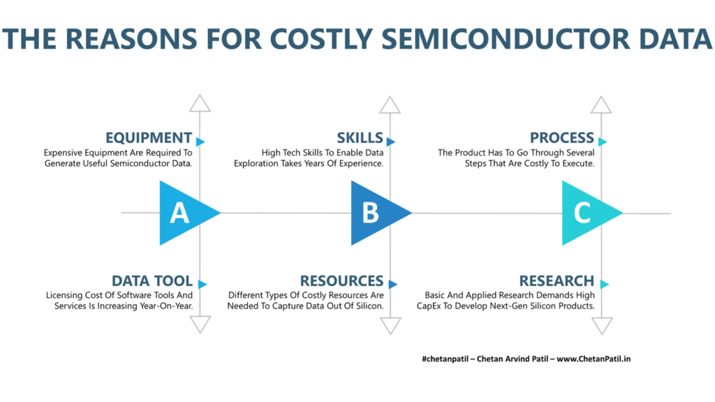
Below is the major reason why the costly semiconductor data is here to stay and how it is also impacting today’s node process and packages out in the market.
Equipment: The different sets of tools and equipment required to drive the successful development of a semiconductor product is key to generating relevant data. Each new design methodology, technology node, and packaging process demands new sets of equipment. This adds to the cost of development and leads to FAB/OSAT upgrade or expansion. This added cost is necessary to ensure that the semiconductor data can be generated and analyzed successfully. Thus showcasing clearly why the semiconductor data cost is on the rise.
Data Tool: The raw data is the first step towards analyzing how the product is behaving on the real silicon. To take a step further, investment is required to procure advanced data analytics tools. The feature-based subscription cost associated with it is also on the rise and is heavily impacting the data analysis part. On top of this, every other year there are a new set of programming solutions that pushes semiconductor data engineers towards a new way of analyzing data. This also requires investment not only in the tool but also in the training and skill upgrade part of it.
Skills: To make the most of the data also demands skills that take years to master. In today’s day and age, the explosion of new technology (on the software side) is also pushing engineers to capture new skill sets on the go. This requires companies to not only invest in core product development resources (FAB to OSAT) but also in people who can explore data with limited information and present the full picture.
Resources: Apart from human resources the data also demands a unique support environment. This can be a factory setup that enables data generation to a data warehouse that is storing all the data-related information. Such resources require a dedicated knowledge team and tools. All the cost associated with such process ends up producing the relevant semiconductor data. Without resources, it is impossible to do any task (not just data exploration).
Process: Technology-node to package to materials (and beyond) all go through a different life cycle and process. This process involves working in a dedicated lab that does require a unique set of tools. To ensure the process are right the tools have to be efficient and the combination of process and tools eventually leads to trustworthy data. The journey of capturing the semiconductor data is thus heavily dependent on these costly processes.
Research: To drive next-gen FETs and XPUs, continuous research is required and it also demands data to validate the new technology/solution. This means a dedicated setup/lab with the next-gen process, equipment, and data tools. All this adds to the costly process of generating the data for research and development activities.
The journey of semiconductor data is very interesting and high-tech. It certainly involves a lot of processes and steps that are dependent on different facilities, equipment, and human resources. As long as the goal is to come up with a new silicon solution, all these semiconductor resources will keep demanding high investment, and in the long run, it is the right thing to do.
The growing importance of semiconductor solutions in every aspect of life is also raising the question as to whether the semiconductor data is the next-gen oil.


