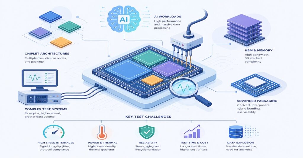
Image Generated With GPT Image 2.0
Evolving Challenges Of Semiconductor Test
Semiconductor testing has always been essential for ensuring quality, reliability, and manufacturing yield. However, the rapid evolution of semiconductor technology is fundamentally changing the nature of production testing. Artificial intelligence accelerators, chiplet architectures, advanced packaging, heterogeneous integration, and high-bandwidth memory are driving unprecedented increases in device complexity.
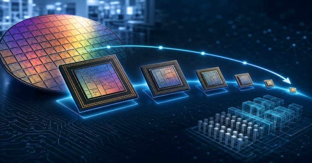
Unlike traditional monolithic devices, today’s semiconductor products often consist of multiple interconnected dies, diverse process technologies, and extremely high-speed interfaces operating within a single package. These innovations deliver remarkable performance improvements but also introduce new challenges throughout the test lifecycle.
As a result, semiconductor test is evolving from a manufacturing checkpoint into a critical enabler of product performance, reliability, and cost optimization.
Key Semiconductor Test Challenges
The complexity of modern semiconductor devices has introduced several challenges that extend well beyond traditional production testing. From chiplet integration and advanced packaging to high-speed interfaces and thermal management, today’s test engineers must validate increasingly sophisticated systems while maintaining high quality, manufacturing throughput, and cost efficiency.
The following table summarizes some of the most significant challenges shaping semiconductor test today and their impact on production test methodologies.
| Challenge | Why It Matters | Impact on Test |
|---|---|---|
| Increasing Device Complexity | AI SoCs integrate CPUs, GPUs, NPUs, HBM, security, and networking on a single platform. | Larger test programs, increased fault coverage requirements, longer validation cycles. |
| Chiplet-Based Architectures | Multiple dies from different process nodes must function as one device. | Requires known-good-die testing, die-to-die interface validation, and package-level verification. |
| Advanced Packaging | 2.5D, 3D stacking, hybrid bonding, and silicon interposers reduce physical access. | Greater dependence on DFT, built-in self-test, boundary scan, and embedded monitoring. |
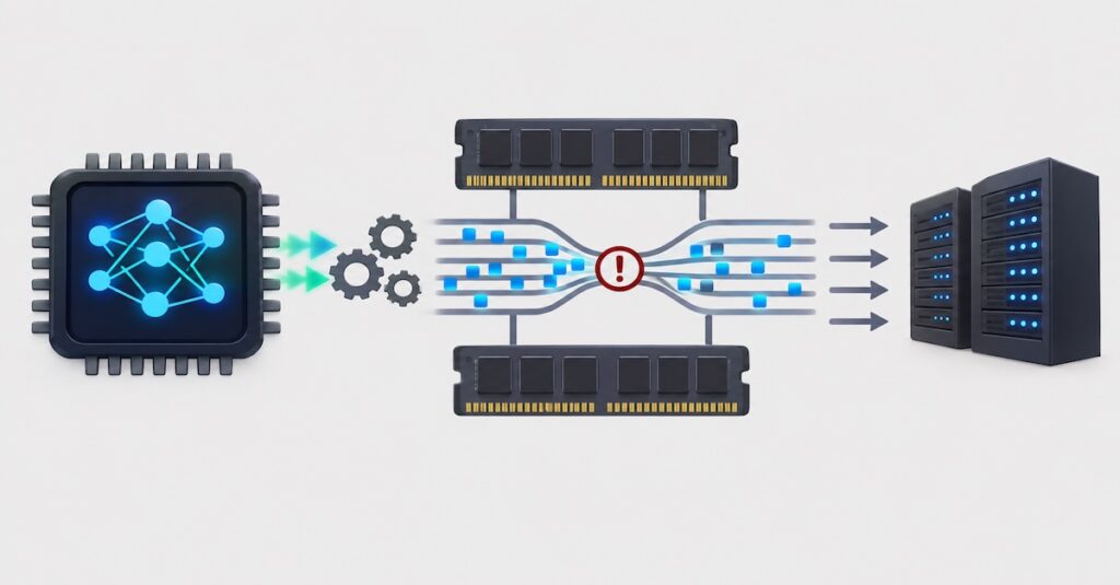
| High-Speed Interfaces | Multi-hundred Gb/s interfaces demand excellent signal integrity. | More complex characterization for timing, jitter, BER, and protocol compliance. |
| Power and Thermal Effects | AI processors consume hundreds of watts under dynamic workloads. | Test conditions must accurately reflect voltage, temperature, and workload variations. |
| Growing Test Cost | Test time increases with device complexity. | Higher manufacturing costs drive optimization through adaptive and data-driven testing. |
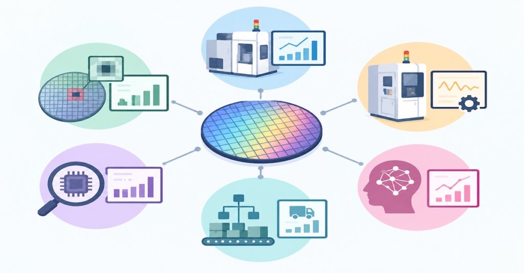
| Data Volume | Modern testers generate enormous amounts of measurement data. | Advanced analytics and AI become necessary for yield learning and failure analysis. |
These challenges are highly interconnected, with advances in one area often creating new complexities in another. For example, chiplet architectures increase the importance of advanced packaging, while higher bandwidth requirements intensify signal integrity and thermal concerns. At the same time, the growing volume of test data and longer production test times place additional pressure on manufacturing costs.
Addressing these challenges requires a combination of improved test methodologies, intelligent automation, standardized interfaces, and closer collaboration between design, packaging, and test engineering teams.
Strategies For Addressing These Challenges
Meeting these challenges requires innovation across the entire semiconductor ecosystem rather than improvements in test equipment alone.
Design-for-Test continues to become more sophisticated, incorporating embedded sensors, built-in self-test, boundary scan, and hierarchical test architectures that improve observability throughout complex devices.
Chiplet-based products increasingly rely on known-good-die methodologies, allowing individual dies to be verified before assembly while reducing the risk of packaging defective components.
Artificial intelligence and machine learning are beginning to optimize production testing by identifying redundant test patterns, predicting failures, improving yield learning, and reducing overall test time without sacrificing quality.
Advanced standards are also playing an increasingly important role by enabling interoperable test access, standardized die-to-die interfaces, and scalable methodologies for heterogeneous integration.
Finally, close collaboration between design, packaging, manufacturing, and test teams enables many test challenges to be addressed much earlier in the product development cycle, reducing both risk and production cost.
Emerging Trends In Semiconductor Test
Several industry trends are expected to shape the future of semiconductor testing.
Test is becoming increasingly system-aware, with validation extending beyond individual dies to complete heterogeneous packages operating under realistic workloads. Production testing is also becoming far more data-centric, leveraging analytics to improve yield, accelerate root-cause analysis, and optimize manufacturing decisions.
The industry is steadily adopting software-defined test platforms that offer greater flexibility as devices continue to evolve. At the same time, AI-assisted test generation and adaptive production testing are reducing test time while maintaining high defect coverage.
As chiplet ecosystems continue to mature, standardized test architectures will become increasingly important for enabling interoperability between components originating from different vendors.