Image Generated With GPT Image 2.0
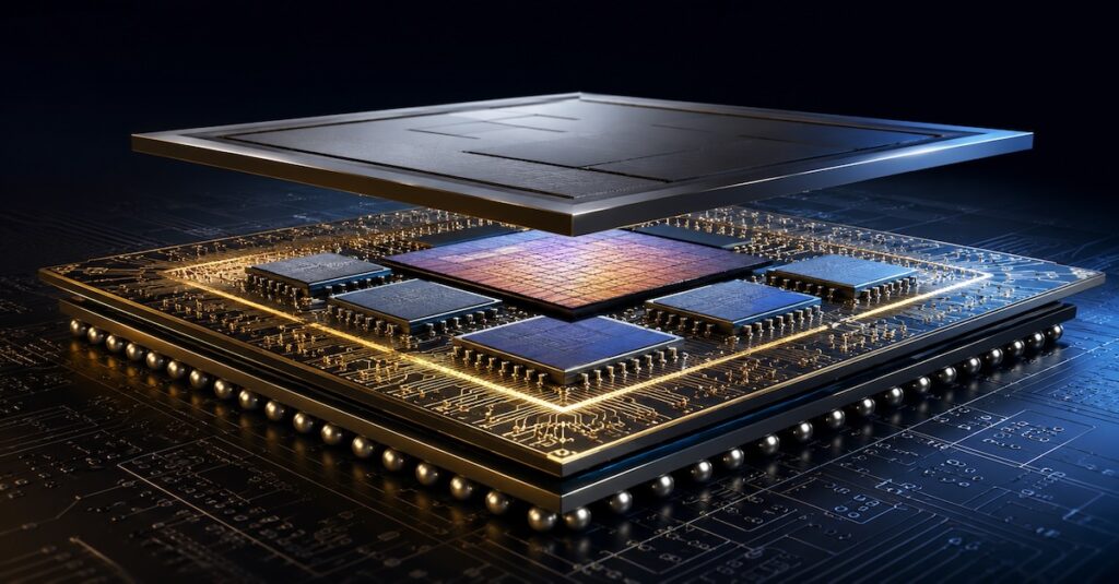
The Amount Of Semiconductor Data Is Exploding
For decades, the semiconductor industry has overcome one bottleneck after another. The focus shifted from transistor density to lithography, from manufacturing capacity to advanced packaging, and more recently to High Bandwidth Memory (HBM) availability and power delivery. While these challenges remain, another bottleneck is quietly emerging that may have an even greater impact on future competitiveness: learning speed.
As semiconductor products become increasingly complex, success is no longer determined solely by how quickly companies can manufacture silicon. It is determined by how quickly they can learn from silicon. Every wafer processed, every package assembled, every test executed, and every deployed device generates engineering knowledge. The team that transform this information into actionable decisions the fastest will accelerate productization, improve yield, and reach production ahead of competitors.
On top, the modern semiconductor manufacturing produces unprecedented volumes of engineering data. Inline process inspection, metrology, wafer sort, package assembly, final test, system-level test, reliability qualification, and field operation all contribute valuable information throughout the product lifecycle.
This growth is occurring alongside increasing product value. AI accelerators are expected to contribute nearly 50% of total semiconductor industry revenue by 2026, despite representing only a small percentage of total unit shipments. Every week saved during yield ramp or qualification can therefore translate into millions of dollars in earlier revenue realization.
Overall, the challenge is no longer collecting more data. Most companies already possess enormous amounts of manufacturing information. The challenge is reducing the time between capturing data and making engineering decisions.
Faster Learning Accelerates Productization
Historically, engineering organizations optimized each manufacturing stage independently. Fabrication focused on process control, assembly optimized packaging, while product engineering concentrated on test yield and quality. Today, those boundaries are disappearing.
Failures observed during final test may originate from lithography variation, package warpage, die-to-die interconnect defects, thermal stress, power delivery instability, or assembly variation. Identifying the root cause requires correlating information across every stage of manufacturing rather than analyzing each process independently.
| Traditional Product Development | Learning-Driven Productization |
|---|---|
| Process optimization | Lifecycle optimization |
| Isolated engineering teams | Connected engineering workflows |
| Historical yield analysis | Predictive yield intelligence |
| Manual failure investigation | Automated root-cause correlation |
| Static test strategies | Adaptive test optimization |
| Learning over months | Learning in near real time |
Industry studies have shown that advanced yield analytics and automated diagnosis can reduce root-cause identification time by 75–90%, significantly shortening yield ramp and accelerating manufacturing maturity. Instead of spending weeks investigating failures, engineering teams can respond within days or even hours.
Learning Speed Is Becoming The New Competitive Advantage
Building an advanced semiconductor fab requires tens of billions of dollars, while advanced packaging capacity and HBM continue to constrain production. Yet capital investment alone no longer guarantees market leadership.
The real differentiator is how quickly organizations convert manufacturing data into engineering knowledge. Faster learning enables earlier design improvements, shorter yield ramps, optimized test programs, faster qualification, higher manufacturing efficiency, and reduced product risk.
In all, the next generation of semiconductor leaders will not simply manufacture silicon faster. They will learn from silicon faster. In an industry where product complexity continues to increase, learning speed is becoming the next critical bottleneck—and ultimately, the next competitive advantage.