The New Semiconductor Fab Is The Package
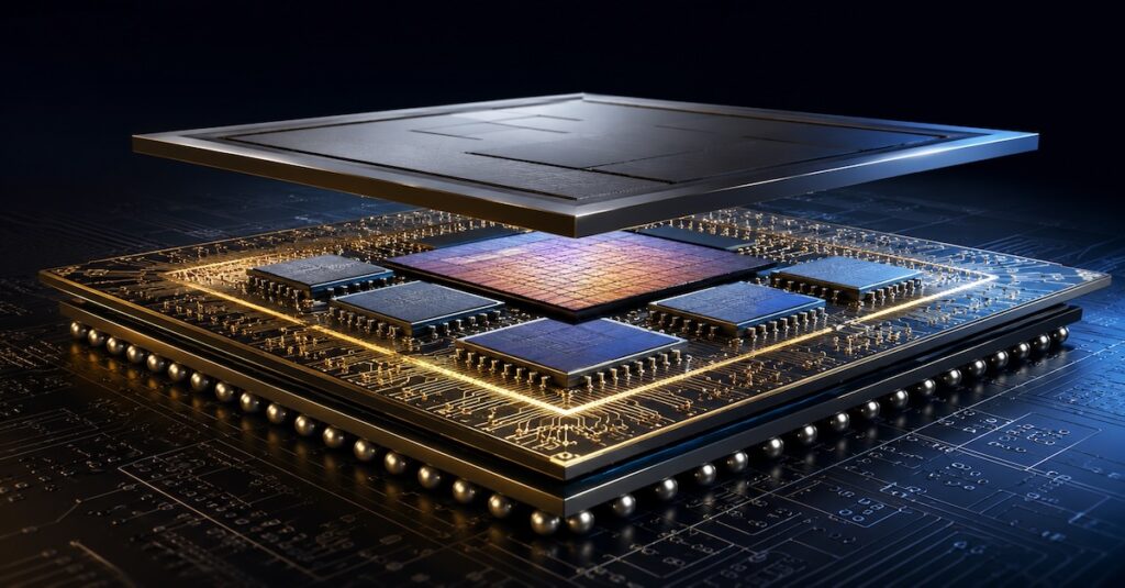
Image Generated With GPT Image 2.0 The Center Of Innovation Is Shifting For decades, semiconductor leadership was defined by transistor scaling and process technology. Performance improvements were achieved by moving to smaller nodes and increasing transistor density, making the fab the primary center of innovation. Today, however, the industry’s biggest challenges are increasingly tied to memory bandwidth, power delivery, thermal management, and data movement, constraints that cannot be solved by transistor scaling alone. As a result, the performance of modern computing systems is becoming increasingly dependent on how efficiently different components are integrated rather than how many transistors can be placed on a single die. This shift is particularly visible in Artificial Intelligence (AI) accelerators, where multiple compute dies, High-Bandwidth Memory (HBM) stacks, advanced substrates, and high-density interconnects must function […]