
Image Generated Using DALL-E
In the fast-paced world of semiconductor product development, two metrics stand out as pivotal to the success and efficiency of manufacturing: yield and test time.
Yield, the percentage of functional chips in a production batch, directly influences the cost-effectiveness and viability of semiconductor products. Simultaneously, test time, the duration spent verifying the functionality and reliability of these chips, plays a crucial role in determining the throughput and overall efficiency of the production process.
Thus, it is essential to understand the intricacies of yield and test time in semiconductor manufacturing, exploring their significance, challenges, and the vital skills required to optimize these critical factors.
Yield In Semiconductor Product Development:
Yield refers to the proportion of functional chips produced from a batch in semiconductor manufacturing. It’s a critical factor in determining the cost-effectiveness of the manufacturing process because higher yields mean more functional chips per batch, reducing the cost per chip.
The complex semiconductor manufacturing process, involving steps like oxidation, coating, lithography, and etching, poses significant yield challenges. Each wafer undergoes hundreds of high-precision processes over three to six months and must pass stringent quality tests.
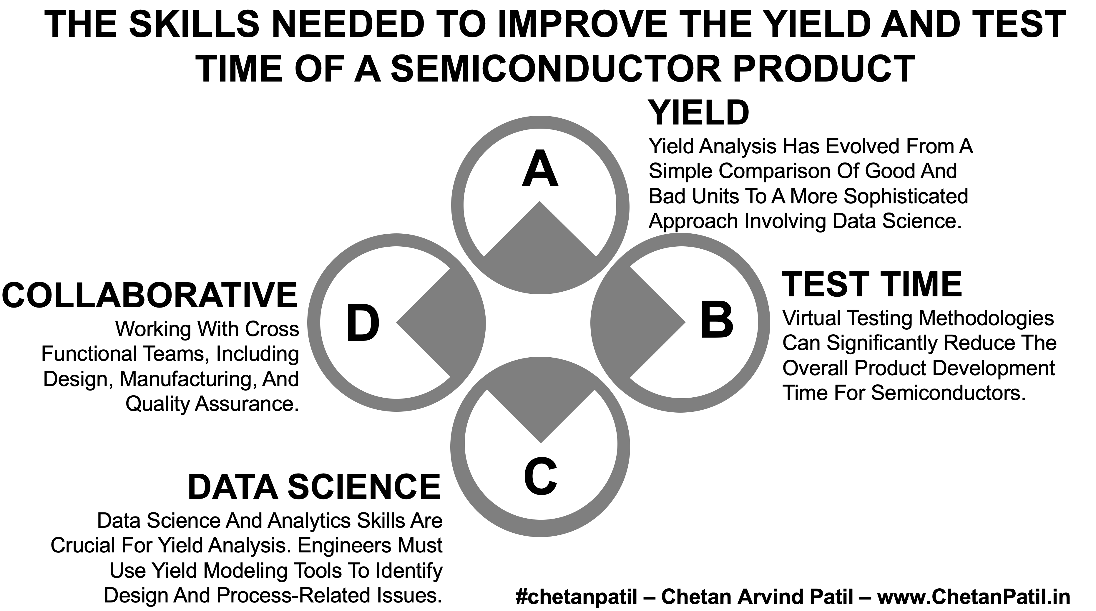
Yield analysis has evolved from a simple comparison of good and bad units to a more sophisticated approach involving data science. This deeper analysis helps in understanding and mitigating a range of factors that contribute to yield issues.
Test Time In Semiconductor Product Development:
Test time in semiconductor manufacturing refers to the duration spent testing the chips for functionality and reliability. Reducing test time is essential for decreasing running costs and improving manufacturing throughput.
Key strategies to reduce test time include eliminating redundant tests, reordering tests to screen out significant failures early, and sample testing or removing “always passing” tests. This approach requires a deep understanding of device behavior.
Virtual testing methodologies can significantly reduce the overall product development time for semiconductors. It allows for earlier detection of potential issues and streamlines the development process.
Skills Needed To Improve Yield And Test Time:
Deep Technical Knowledge: Understanding the intricate details of semiconductor manufacturing processes and the behavior of devices is essential. This knowledge enables engineers to identify and address yield issues effectively and to streamline testing processes.
Data Analysis And Yield Modeling: Data science and analytics skills are crucial for yield analysis. Engineers must use yield modeling tools to identify design and process-related issues.
Design For Testability (DFT) Expertise: Engineers should have expertise in designing chips with testability in mind. It involves creating more straightforward test and diagnose designs, thus improving yield and reducing test time.
Process Optimization: Skills in process optimization, removing redundant steps in manufacturing and testing, are vital. It includes reengineering test flows and optimizing test programs.
Familiarity With Virtual Testing Tools: Knowledge of virtual testing methodologies and tools can help reduce product development time and early issue detection.
Adaptability To Technological Advances: As semiconductor technology evolves, staying updated with the latest methodologies and tools is crucial for continuous yield and test time improvement.
Collaborative Skills: Working effectively with cross-functional teams, including design, manufacturing, and quality assurance, is essential for holistic improvements in yield and test time.
In conclusion, mastering the aspects of yield and test time is indispensable in the realm of semiconductor manufacturing. The journey from understanding the complexities of these factors to effectively implementing strategies for improvement requires a blend of technical acumen, analytical prowess, and innovative thinking.
Professionals in the field must continually evolve, embracing new methodologies and technologies to stay ahead in this dynamic industry. The enhancement of yield and test time bolsters production efficiency and serves as a cornerstone for the business success and technological advancement of semiconductor products.


