Image Generated Using 4o
The semiconductor industry is at an inflection point. For decades, the trajectory of Moore’s Law provided a predictable path forward: smaller transistors, higher performance, and lower costs. But as I discussed in The More Than Moore Semiconductor Roadmap, shrinking nodes alone can no longer sustain the pace of progress. Physical and economic limits are forcing the industry to seek new strategies that redefine what advancement means in this post-Moore era.
Two of the most important forces reshaping the landscape are chiplets and artificial intelligence.
Chiplets provide modularity, efficiency, and flexibility in system design, while AI is driving entirely new computational demands and design paradigms. Each of these trends is powerful on its own, but their true potential emerges when considered together. The convergence of chiplets and AI is setting the foundation for how future semiconductors will be conceived, validated, and manufactured.
Why Chiplets And AI
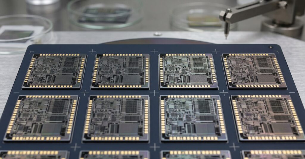
Chiplets break down large monolithic SoCs into smaller, reusable building blocks that can be integrated within a package. This approach reduces reticle size constraints, improves yield, and allows system designers to mix different process nodes and IP blocks. As explained in The Rise of Semiconductor Ghiplets, modularity is not just about performance scaling but also about lowering costs and accelerating time to market.
AI, on the other hand, is creating workloads that are unprecedented in size and complexity. Training neural networks with billions of parameters requires not just raw compute power, but also immense memory bandwidth, efficient data movement, and specialized accelerators.
These demands are increasingly challenging to meet with monolithic designs. Chiplets solve this by allowing designers to integrate AI accelerators, memory dies, and I/O blocks within the same package, scaling systems in ways monolithic chips cannot.
The relationship is symbiotic. AI workloads need chiplets for modular scalability, while chiplets need AI to push the development of advanced architectures, packaging, and simulation tools that can handle the complexity of integration.
AI Needing New Chiplet Based Architecture
The rapid scaling of AI models has exposed the limitations of traditional semiconductor design. As explored in The Hybrid AI and Semiconductor Nexus, AI is forcing the industry to rethink architectures around data movement, memory hierarchies, and workload-specific optimization. Monolithic SoCs struggle to deliver the balance of compute and bandwidth that AI requires.
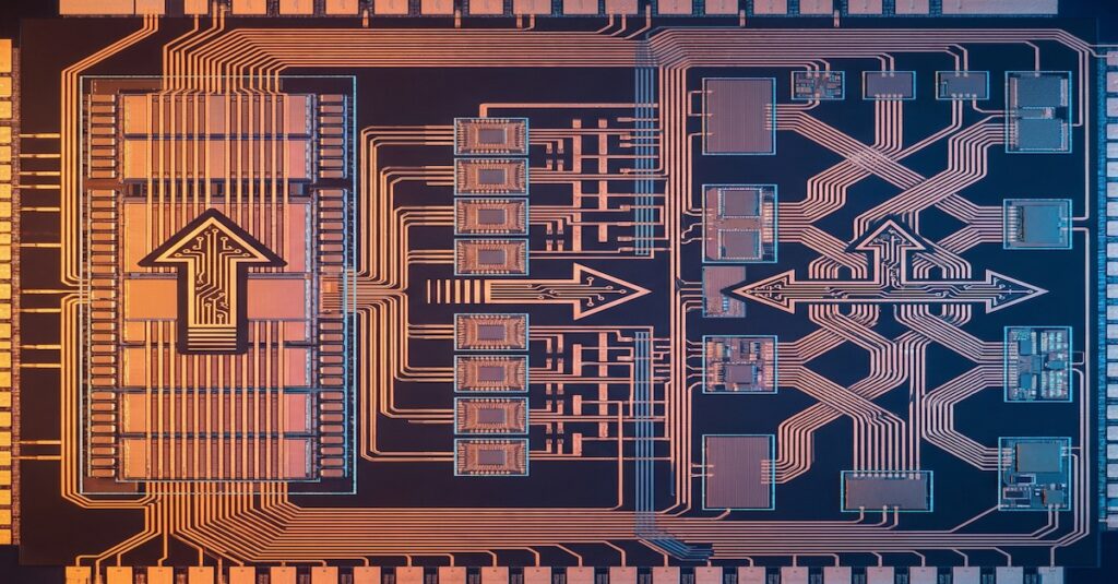
Chiplet-based architectures solve this by enabling heterogeneous integration. A single package can combine logic dies manufactured on cutting-edge nodes with memory chiplets on mature nodes and I/O dies optimized for high-speed connectivity. This modularity allows for greater flexibility in designing AI accelerators tailored to specific workloads, whether in data centers, edge devices, or mobile platforms.
Industry standards like UCIe are accelerating this shift by providing open, vendor-neutral interconnects that make chiplet ecosystems interoperable. This means AI hardware development no longer needs to rely on closed, vertically integrated designs, but can instead draw from an ecosystem of interoperable components. Without chiplets, scaling AI hardware efficiently would be economically unsustainable.
Bottleneck For AI And Chiplets To Grow Together
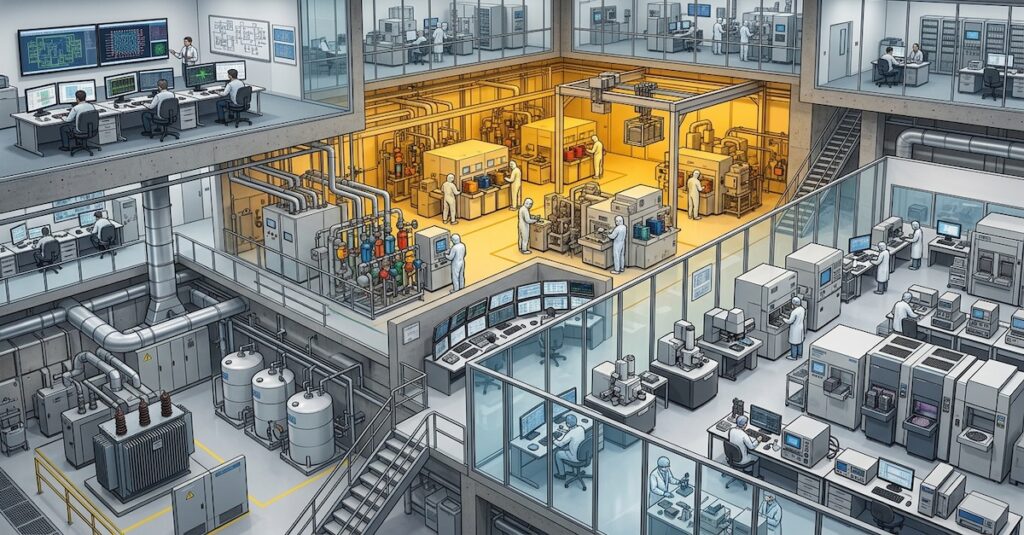
Despite the promise, the convergence of chiplets and AI faces significant bottlenecks. Packaging complexity is one of the most pressing. High-speed die-to-die interconnects must be validated for signal integrity across process, voltage, and temperature corners. In 2.5D and 3D packages, thermal gradients create hotspots that impact performance and reliability. Mechanical stresses from advanced packaging compounds must also be modeled to avoid long-term failures. These are not trivial extensions of SoC verification, but entirely new domains of system-level engineering.
Yield is another critical constraint. As I explained in The Economics of Semiconductor Yield, profitability in semiconductors depends heavily on how many functional dies come off a wafer. With chiplets, the probability of system-level failure increases since multiple dies must work together flawlessly. A defect in one chiplet can compromise an entire package, multiplying yield risks. This is why embedding yield optimization into the design process is so essential.
Finally, simulation and validation remain major bottlenecks. As noted in The Role of Simulation in Semiconductor Product Development, traditional EDA flows were not designed to handle chiplet-level interactions. AI-driven simulation, as I explored in The Semiconductor Data Driven Decision Shift, offers a path forward. However, the industry is still in the early stages of building predictive, adaptive simulation environments capable of handling such complexity.
The convergence of chiplets and AI is not a coincidence but a necessity. AI workloads demand architectures that can only be delivered through modular chiplet design. At the same time, chiplets require the intelligence and predictive power of AI-driven simulation to overcome integration and yield challenges.
As I discussed in The Semiconductor Learning Path, success in the post-Moore era requires connecting design, manufacturing, and data into a unified roadmap. Chiplets and AI are two of the most critical pillars in this roadmap, and their convergence is redefining how the industry balances complexity, cost, and scalability.
The companies that master this interplay will not only meet the demands of today’s AI workloads but also shape the semiconductor roadmaps of the next decade. The future of design is modular, data-driven, and inseparable from the intelligence that AI brings to every stage of the value chain.