Image Generated With GPT Image 2.0
The Center Of Innovation Is Shifting
For decades, semiconductor leadership was defined by transistor scaling and process technology. Performance improvements were achieved by moving to smaller nodes and increasing transistor density, making the fab the primary center of innovation.
Today, however, the industry’s biggest challenges are increasingly tied to memory bandwidth, power delivery, thermal management, and data movement, constraints that cannot be solved by transistor scaling alone. As a result, the performance of modern computing systems is becoming increasingly dependent on how efficiently different components are integrated rather than how many transistors can be placed on a single die.
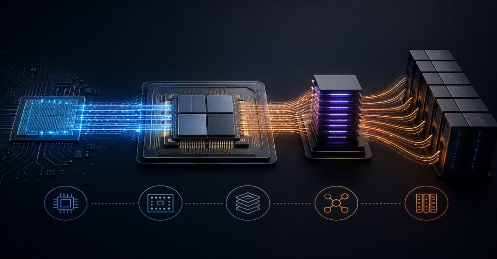
This shift is particularly visible in Artificial Intelligence (AI) accelerators, where multiple compute dies, High-Bandwidth Memory (HBM) stacks, advanced substrates, and high-density interconnects must function as a single system.
Consequently, competitive advantage is no longer determined solely by process-node leadership but also by the ability to integrate, power, cool, and manufacture complex heterogeneous packages at scale. Innovation is expanding beyond the wafer fab and into the package, where system-level performance, scalability, and manufacturing efficiency are increasingly determined.
The Package Has Become A System Integration Platform
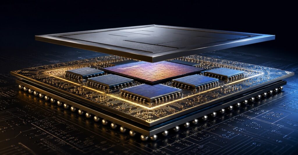
The role of semiconductor packaging has evolved far beyond protecting and connecting a silicon die. Modern packages have become system integration platforms that bring together compute, memory, networking, and specialized accelerators into a single functional unit.
This transition has been driven by the growing demand for higher performance and bandwidth, particularly in Artificial Intelligence (AI) and high-performance computing applications.
Technologies such as silicon interposers, embedded bridges, fan-out architectures, and three-dimensional stacking enable thousands of high-density connections between multiple dies and High-Bandwidth Memory (HBM) stacks.
These package-level interconnects enable designers to overcome the reticle-size limitations of advanced nodes while optimizing performance, power efficiency, and manufacturing yield. As a result, many of the architectural decisions that once occurred at the silicon level are now being made at the package level, making advanced packaging a critical enabler of next-generation computing systems.
Manufacturing Challenges Are Moving Beyond The Die
As semiconductor architectures become increasingly disaggregated, manufacturing complexity extends well beyond wafer fabrication. Yield is no longer determined solely by transistor performance and process control within a single die.
Instead, the final product yield depends on the successful integration of multiple dies, High-Bandwidth Memory (HBM) stacks, advanced substrates, interconnect structures, and assembly processes. Every additional component and manufacturing step introduces new opportunities for defects, variability, and reliability concerns.
Advanced packages require precise die placement, fine-pitch interconnect formation, substrate flatness control, warpage management, and thermal-mechanical stress optimization throughout the assembly flow. Engineers must also validate die-to-die interfaces, power delivery networks, signal integrity, and package-level thermal behavior before the product reaches system-level testing.
Consequently, yield learning now extends across wafer fabrication, assembly, packaging, test, and system validation. The challenge is no longer simply producing a functional die, it is manufacturing a complete heterogeneous system that can meet performance, power, reliability, and quality requirements at production scale.
The New Scaling Engine
For decades, the semiconductor industry relied on transistor scaling as the primary mechanism for improving performance and reducing cost per function. While process technology remains important, the economics and complexity of advanced nodes are making it increasingly difficult to achieve system-level gains through silicon scaling alone.
As a result, the industry is adopting a broader approach where performance improvements are delivered through heterogeneous integration, advanced packaging, and system-level optimization.
| Traditional Scaling Model | System-Level Scaling Model |
|---|---|
| Performance driven by smaller transistors | Performance driven by heterogeneous integration |
| Monolithic System-on-Chip (SoC) architectures | Chiplet-based architectures |
| Process node as primary differentiator | Package architecture as a key differentiator |
| Scaling through transistor density | Scaling through compute, memory, and I/O integration |
| Yield optimized at die level | Yield optimized across the entire system |
| Limited by reticle size and die area | Flexible scaling through multiple interconnected dies |
| Value concentrated in wafer fabrication | Value distributed across fabrication, packaging, and assembly |
| Node migration drives performance gains | System architecture drives performance gains |
This transition does not signal the end of transistor scaling. Rather, it expands the industry’s scaling toolkit. Future semiconductor leadership will increasingly depend on the ability to combine advanced silicon, memory, packaging, power delivery, thermal management, and manufacturing technologies into a cohesive system.
In many ways, the package has become the new scaling engine, enabling performance improvements that would be difficult or economically impractical to achieve through silicon alone.