Image Generated With GPT Image 2.0
Semiconductor Scaling Is Becoming A System Problem
The semiconductor industry is entering a phase in which scaling is no longer defined solely by transistor density. For decades, advances in lithography and process scaling have improved performance, power efficiency, and integration density. Smaller transistors enabled greater computing capability within the same silicon area, supporting the growth of cloud computing, mobile devices, and artificial intelligence systems.
That model is now under increasing pressure. Advanced nodes continue to improve transistor density, but the system-level benefits no longer scale linearly. Power density has become more difficult to manage, reticle size limitations constrain die growth, and manufacturing complexity continues to rise. At the same time, AI workloads are reshaping compute infrastructure by demanding massive data movement across processors, memory systems, storage, and networking fabrics.
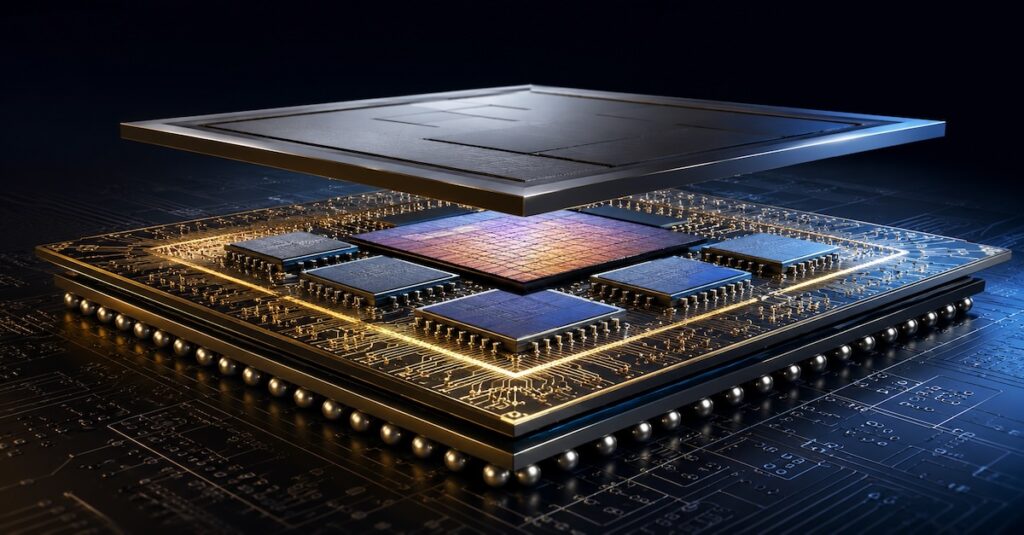
This shift has exposed a broader challenge. Semiconductor scaling is increasingly constrained not only by the ability to compute, but by the ability to move data efficiently across the system. As architectures become more distributed through chiplets, heterogeneous integration, and disaggregated infrastructure, communication overhead increasingly dominates performance.
The table above reflects a broader transition occurring across the semiconductor industry. Systems are no longer isolated compute devices. Packaging, networking, memory hierarchy, and communication infrastructure are increasingly determining overall system performance.
| Scaling Dimension | Traditional Semiconductor Scaling | Emerging AI Infrastructure Scaling |
|---|---|---|
| Primary Objective | Increase transistor density | Increase communication efficiency |
| Dominant Constraint | Lithography scaling | Data movement and power |
| System Structure | Monolithic SoC | Chiplets and heterogeneous systems |
| Communication Model | Electrical interconnects | Hybrid electrical and optical fabrics |
| Performance Bottleneck | Compute throughput | Bandwidth and latency |
Historically, electrical interconnects were sufficient for communication within semiconductor systems. However, the scale of AI infrastructure is pushing copper-based signaling toward physical and economic limits. Signal degradation increases over distance, power consumption rises with bandwidth scaling, and thermal constraints become increasingly difficult to manage in dense compute environments.
The industry response has been a shift from monolithic to system-level scaling. Advanced packaging technologies such as chiplets, 2.5D integration, and 3D stacking enable designers to distribute functions across multiple dies, improve yield, and enable heterogeneous integration. These approaches extend scaling, but they also increase communication complexity because data must move efficiently between a growing number of compute elements.
This transition creates what can be described as the semiconductor scaling trilemma.
Silicon Photonics As A Scaling Architecture
This environment is creating the conditions for silicon photonics to emerge as a strategic scaling technology. Instead of relying entirely on copper-based electrical interconnects, silicon photonics uses light to transmit data with lower signal loss and improved energy efficiency across longer distances.
Its importance lies in addressing one of the central limitations of modern semiconductor scaling: the rising cost of data movement. As bandwidth requirements increase, electrical interconnects face rising resistance, thermal overhead, and signal integrity challenges, particularly in large-scale AI systems where communication patterns are highly distributed.
Optical communication provides several advantages in this environment. Light can carry larger amounts of data across longer distances while supporting higher bandwidth density without proportionally increasing power consumption. This makes silicon photonics increasingly attractive for AI clusters, data center fabrics, and co-packaged infrastructure.
The transition toward silicon photonics is already visible through co-packaged optics, optical I/O architectures, and photonic integrated circuits. Importantly, silicon photonics does not replace conventional semiconductor scaling. Instead, it complements it by addressing communication limitations that electrical scaling alone cannot solve efficiently.
This represents a major shift for the semiconductor industry. Future scaling may depend less on transistor density alone and more on efficiently moving information across increasingly distributed systems.