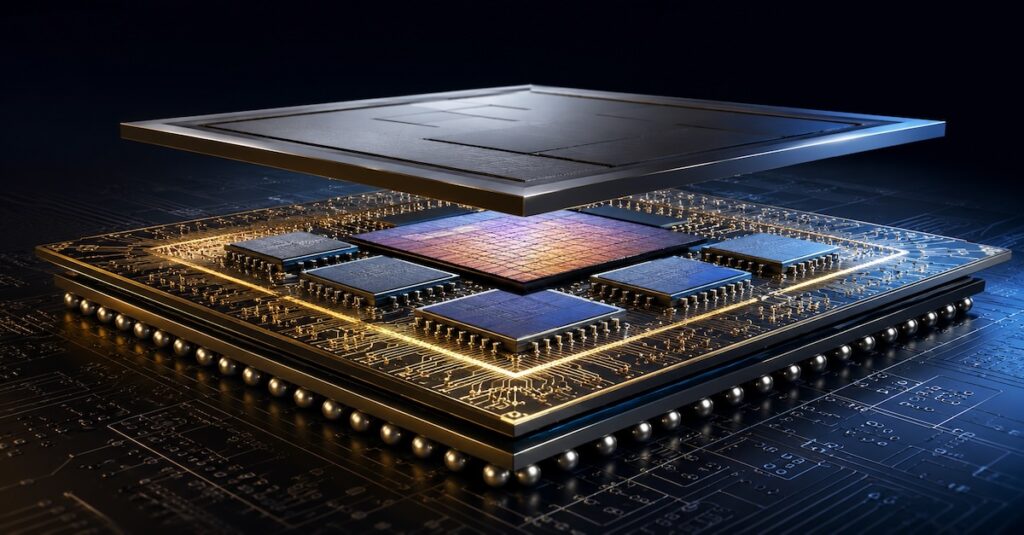
Image Generated Using Nano Banana
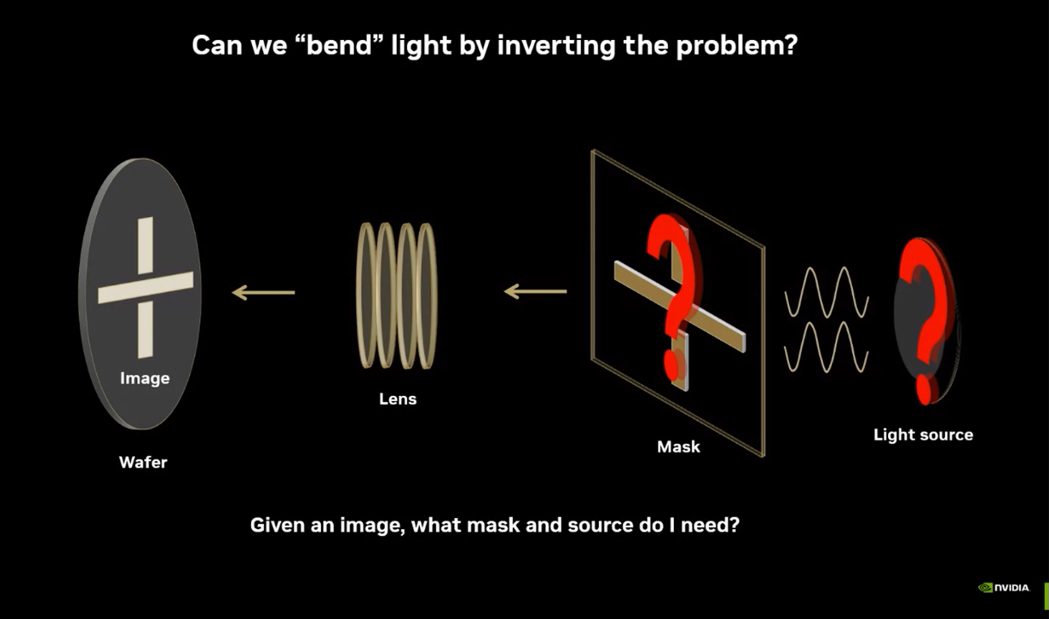
From Optical Limits To Computational Correction
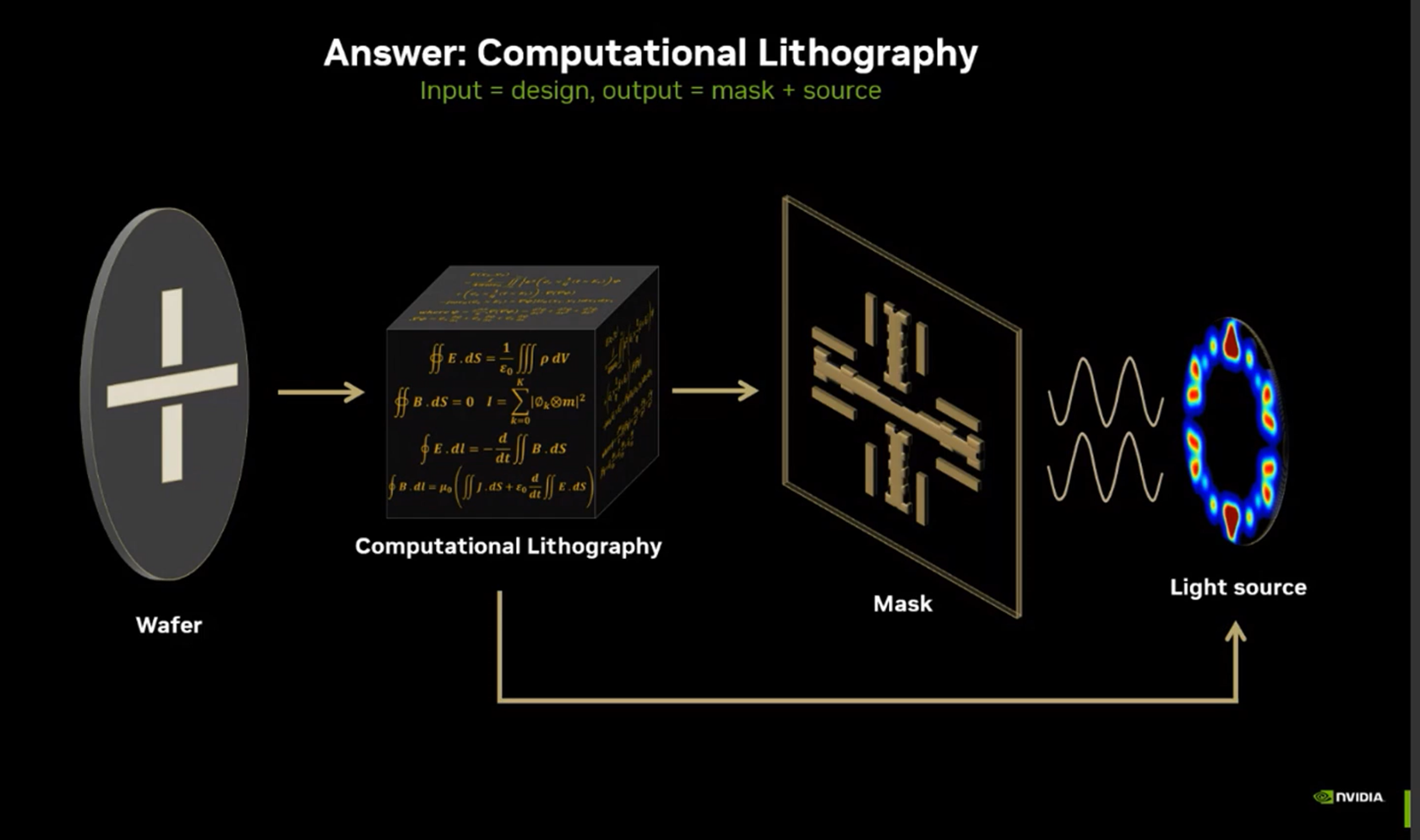
Computational lithography has become central to advanced semiconductor manufacturing. Traditional optical scaling is reaching its physical limits. At nanometer dimensions, patterns designed on masks cannot be directly transferred onto silicon with sufficient fidelity. This is due to diffraction, interference, and process variability. The gap between intended design and printed structure must be corrected before fabrication begins.
This correction is not a simple adjustment. Instead, it is a computational transformation. Mask patterns are intentionally modified to counteract known distortions. These adjustments ensure that the final silicon structure matches design intent. As a result, lithography is no longer just a process step. It is a predictive, optimization-driven system that operates before and during manufacturing.
Mastery in computational lithography requires understanding how multiple domains interact. It is not defined by a single skill. It relies on the ability to connect physics, mathematical modeling, algorithmic techniques, and manufacturing constraints. All of these elements must form a unified workflow. This integrated perspective forms the foundation of the computational lithography stack.
Domains And Their System Impact
Computational lithography can be understood as a structured stack of capabilities, where each domain contributes directly to pattern fidelity, manufacturability, and yield. The effectiveness of the overall system depends on how well these domains are integrated.
This table highlights that computational lithography is fundamentally about pre-compensating for physical reality through computation, while ensuring that solutions remain scalable and manufacturable.
| Domain | Core Knowledge | Methods And Techniques | System Impact |
|---|---|---|---|
| Physical Foundations | Optical imaging, diffraction, EUV behavior, resist interaction | Imaging models, process characterization | Defines resolution limits and pattern distortions |
| Mathematical Modeling | Numerical methods, inverse problems, electromagnetic simulation | Lithography simulation, compact models | Enables predictive understanding of wafer outcomes |
| Algorithmic Techniques | Optimization theory, computational geometry | OPC, SMO, ILT | Drives correction of mask patterns to match design intent |
| Compute Infrastructure | Parallel computing, HPC, GPU acceleration | Distributed simulation, accelerated solvers | Determines runtime, scalability, and cost efficiency |
| Manufacturing Integration | Process window, variability, yield analysis | Mask synthesis, process validation | Ensures solutions translate into high volume production |
Each domain operates within a feedback-driven system rather than as an isolated function. For example, physical models inform algorithmic corrections, while manufacturing data refines those models. Similarly, compute capabilities influence the level of model complexity that can be practically deployed.
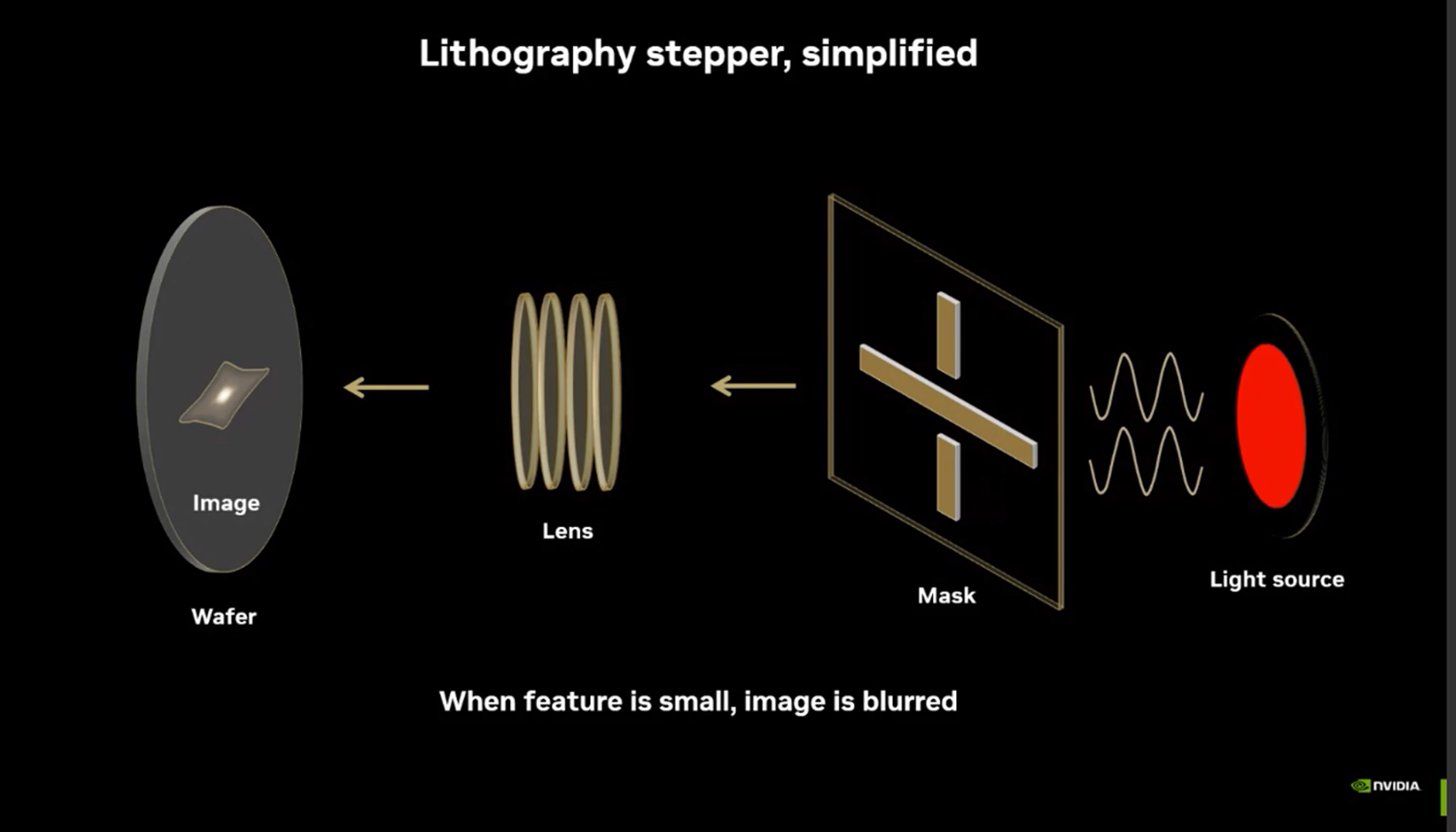
Image Source: NVIDIA
Interdependence Across The Stack
In short, computational lithography is characterized by strong coupling across domains, in which decisions in one layer directly affect the entire system. Physical modeling sets the limits of pattern transfer by capturing optical behavior, resist effects, and process interactions. Incomplete models lead to physically invalid corrections, while highly detailed models improve accuracy but increase computational cost, creating a balance between fidelity and efficiency.
Algorithmic techniques solve inverse problems that map target wafer patterns to mask geometries. Methods such as Optical Proximity Correction and Inverse Lithography Technology rely on iterative optimization across nonlinear design spaces. Their effectiveness depends on model accuracy and computational efficiency, which require trade-offs in convergence, runtime, and scalability.
Compute infrastructure enables these methods at scale. Full-chip simulations demand distributed systems and acceleration, which influence how models are simplified and algorithms are parallelized. Computational lithography, therefore, is both an algorithmic and a high-performance computing problem.
Manufacturing integration validates the entire flow. Corrections must remain robust across variations in focus, dose, and materials. Feedback from wafer inspection and test refines models and algorithms, ensuring alignment between prediction and silicon. This interdependence requires system-level thinking across the full pipeline
The Path And Future Direction
Mastery in computational lithography requires the ability to integrate the full stack rather than operate within a single domain. Engineers need depth in one area, supported by working knowledge across physics, modeling, algorithms, computing, and manufacturing to enable system-level optimization.
The learning path typically progresses from fundamentals in physics and semiconductor processes to mathematical modeling and simulation. This is followed by algorithm development and exposure to computing systems for large-scale optimization. Experience with manufacturing flows and yield analysis ultimately connects theory to silicon outcomes.
The field is evolving as design complexity increases and iteration requirements become faster. Machine learning is being introduced to augment physics-based methods through surrogate models, improving prediction speed and reducing reliance on full simulations in select workflows.
At the same time, advances in computing platforms are enabling higher performance and scalability. This supports more detailed simulations and broader design exploration, improving pattern fidelity and process robustness.
Despite these changes, the core objective remains the same. Computational lithography bridges the gap between design intent and manufacturing reality. Success depends on how effectively this integration is executed across domains.