Image Generated Using Nano Banana
From Strategy To Necessity
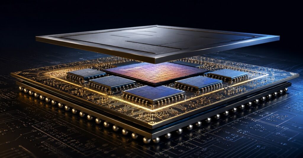
As technology continues to shape every aspect of modern life, dependence on semiconductor solutions has grown from a convenience into critical infrastructure. Semiconductors power everything from sensors and smartphones to automobiles, cloud platforms, and advanced computing systems, making them foundational to modern digital experiences.
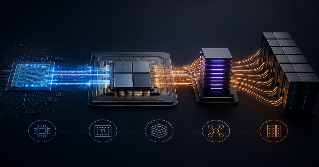
Among the most important systems enabled by semiconductor innovation are data centers and portable computing devices. These two ecosystems operate in a tightly coupled cycle, in which every request from a mobile or edge device ultimately relies on large-scale data center infrastructure to process, compute, and deliver results. As software adoption expands, AI workloads increase, and data generation accelerates, the demand for efficient and purpose-built computing solutions has reached unprecedented levels.
Several years ago, developing custom semiconductor chips in-house was primarily viewed as a strategic differentiator pursued by a select group of technology leaders. Today, that perspective has evolved.
Thus, in-house semiconductor development is increasingly becoming a structural shift in how data-driven companies design, optimize, and deploy their computing platforms to achieve long-term scalability and competitive advantage.
Data-Driven Companies Entering Semiconductor Development
Traditionally, large software and data-centric companies relied on established semiconductor vendors providing general-purpose solutions. These processors were designed to serve a wide customer base and delivered strong scalability for many years.
However, as data volumes expanded and workloads became more specialized, limitations of the general-purpose approach began to appear. Companies operating large-scale infrastructure realized that many of their performance bottlenecks were tied to silicon decisions that were outside their direct control.
This realization triggered a major industry shift.
Instead of adapting software to available hardware, organizations began designing hardware that aligned directly with their software and service requirements. Examples across the industry demonstrate how custom silicon enables optimized workloads, ranging from video processing acceleration to secure platform architectures, proving that internal silicon design can directly improve system efficiency and overall user experience.
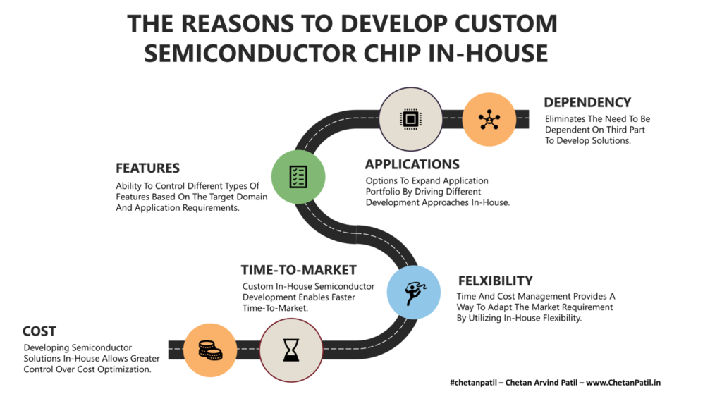
The Core Reasons Behind In-House Chip Development
The motivations behind in-house semiconductor development have not disappeared, they have evolved. What began as a response to performance, cost, and dependency challenges has matured into a broader strategic model where silicon decisions directly influence platform architecture, software efficiency, and long-term business agility.
The table below highlights how the original drivers of custom chip development have transformed as the industry moved from the first wave of in-house silicon toward today’s platform-centric approach.
| Driver | First Wave (Early In-House Development) | Current Evolution (Custom Silicon 2.0) |
|---|---|---|
| Cost | Focus on reducing hardware procurement and power costs through custom optimization | System-level efficiency including power, workload utilization, and total infrastructure economics |
| Time-to-Market | Greater control over product launch cycles compared to external silicon roadmaps | Synchronization of silicon, software, and service deployment for faster platform innovation |
| Flexibility | Ability to add specific features required by internal software teams | Continuous hardware–software co-design enabling rapid iteration and adaptive architectures |
| Features & Differentiation | Custom features to avoid dependency on generic solutions | Strategic feature ownership driving competitive platform advantages |
| Applications | Enable new product categories by tailoring silicon to use cases | Creation of scalable compute ecosystems supporting AI, cloud, and edge workloads |
| Dependency | Reduce reliance on external semiconductor vendors | Long-term architectural independence and stronger control over innovation direction |
This evolution shows that in-house semiconductor development is no longer simply about designing a better chip. It has become a mechanism for aligning silicon strategy with business outcomes, enabling organizations to build tightly integrated compute platforms where hardware, software, and data evolve together. The shift from component thinking to ecosystem thinking ultimately defines the next phase of custom silicon development.
The Future of Custom Silicon
In-house semiconductor development has moved far beyond its early role as a cost or performance optimization exercise. It now represents a strategic foundation for how modern technology companies build, scale, and differentiate their computing platforms. As software workloads grow more complex, data volumes expand, and AI-driven applications redefine infrastructure requirements, silicon decisions increasingly influence the entire technology stack.
Organizations are no longer viewing chips as isolated components but as integral elements of a larger ecosystem where architecture, software frameworks, data pipelines, and operational intelligence evolve together. This shift reflects a deeper alignment between hardware design and long-term platform strategy, enabling companies to create more efficient, purpose-built computing environments.
This evolution also reflects a broader industry realization that long-term competitiveness depends on controlling the points where hardware and software intersect. Companies that invest in internal semiconductor capabilities gain not only technical flexibility but also the ability to align innovation cycles with business goals, accelerate product development, and respond faster to changing market demands.
While not every organization needs to develop silicon in-house, those that strategically integrate semiconductor thinking into their platform vision are better positioned to create scalable, efficient, and future-ready solutions. The next chapter of custom silicon development will therefore be defined not just by better chips, but by the ability to build intelligent, adaptive computing ecosystems that continuously learn and improve over time.