Published By: Silicon India
Date: 14th June 2024
Media Type: Digital
Optimizing Semiconductor Product Development: Chetan Arvind Patil On Yield, Testing, And Industry Impact
- | Published On:
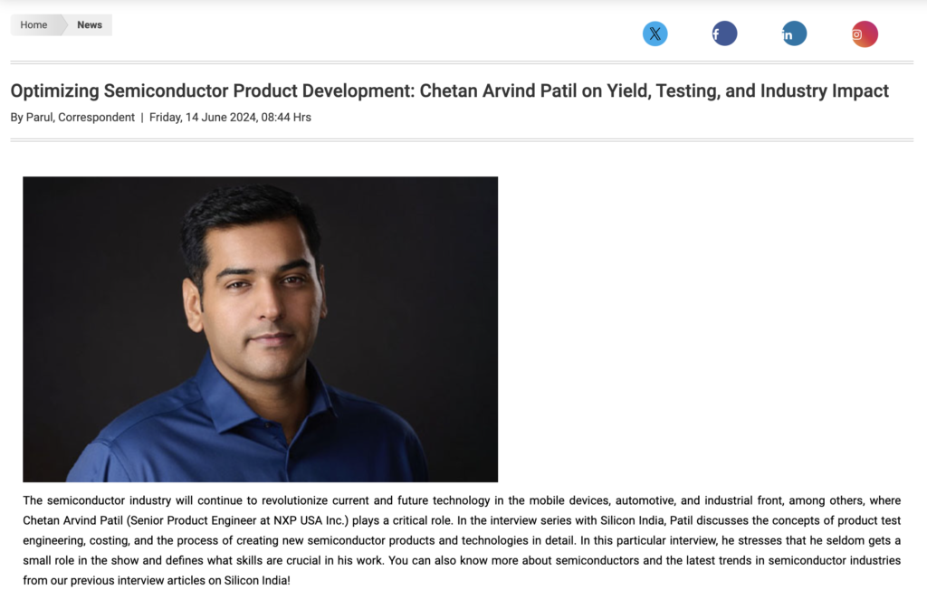

Chetan Arvind Patil
Hi, I am Chetan Arvind Patil (chay-tun – how to pronounce), a semiconductor professional whose job is turning data into products for the semiconductor industry that powers billions of devices around the world. And while I like what I do, I also enjoy biking, working on few ideas, apart from writing, and talking about interesting developments in hardware, software, semiconductor and technology.
COPYRIGHT
2026
, CHETAN ARVIND PATIL
This work is licensed under a Creative Commons Attribution-NonCommercial-ShareAlike 4.0 International License. In other words, share generously but provide attribution.
DISCLAIMER
Opinions expressed here are my own and may not reflect those of others. Unless I am quoting someone, they are just my own views.
RECENT POSTS

Image Generated With GPT Image 2.0 The Center Of Innovation Is Shifting For decades, semiconductor leadership was defined by transistor

Image Generated With GPT Image 2.0 Data Is Becoming A Strategic Investment For decades, semiconductor investments have focused on fabs,

Image Generated With GPT Image 2.0 Compute Scaling Alone Is No Longer Enough For decades, semiconductor progress was driven primarily

Image Generated With GPT Image 2.0 State Of Silicon Agents Artificial intelligence in semiconductors is rapidly moving beyond copilots and

Image Generated With GPT Image 2.0 System-Level Scaling Beyond Moore’s Law The semiconductor industry is moving beyond traditional transistor scaling.