Image Generated Using 4o
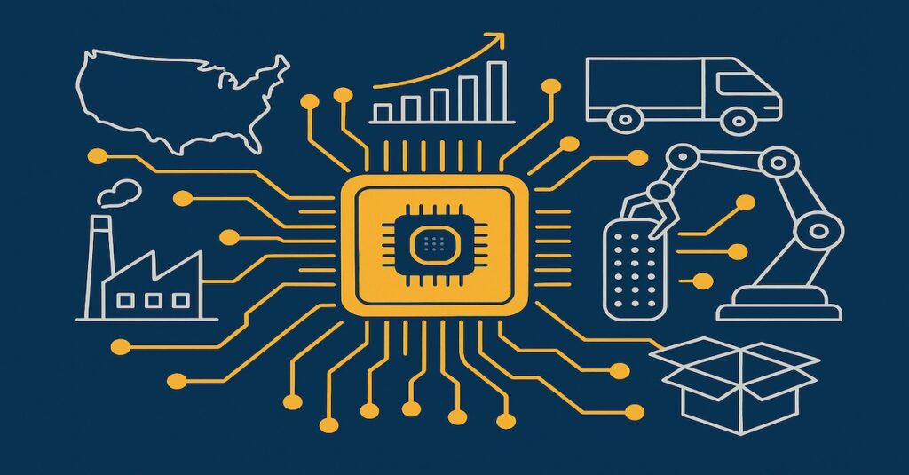
United States Semiconductor Industry
The United States semiconductor industry has been foundational in shaping the modern digital world. From the invention of the integrated circuit to the articulation of Moore’s Law, the U.S. was instrumental in pioneering the core technologies that underpin global electronics today.
However, as we enter 2025, the landscape has shifted. While the U.S. continues to lead in critical upstream segments, including chip design, electronic design automation (EDA), and semiconductor manufacturing equipment, much of its physical fabrication and packaging capability has migrated overseas over the course of last four decades. The result is a complex mix of strength in innovation and dependency in production.
To understand the current position and emerging trajectory of the U.S. semiconductor supply chain, it is thus essential to examine it across four interdependent domains:
- Manufacturing And Packaging Capabilities
- Upstream Leadership: Equipment, EDA, And IP
- Policy, Industrial Strategy, And The CHIPS Act
- The Road Ahead: Building A Resilient And Competitive Future
Each domain highlights not only the past’s legacy and limitations but also the strategic imperatives shaping the next chapter of U.S. semiconductor leadership.
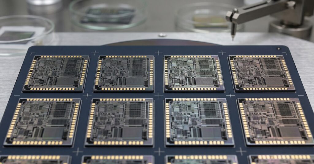
Manufacturing And Packaging Capabilities
Over 80 percent of global semiconductor packaging is now carried out in Asia by Outsourced Semiconductor Assembly and Test (OSAT) providers. Although there are OSATs that are headquartered in the United States, most of its packaging (manufacturing plants) operations are based in Asian countries.
Historically, the United States pioneered packaging technologies, from dual in-line packages to early wire bond methods. However, by the late 1990s, these labor-intensive processes had largely been offshored. Today, chips are designed in the U.S., and at the same time the fabrication is overseas and only returned as completed parts ready for system integration.
This structural dependency is becoming more critical as the packaging itself transitions from a cost center to a performance enabler. The emergence of advanced packaging, such as 2.5D interposers, chiplet-based architectures, and three-dimensional stacking, redefines the backend’s role in overall system performance. These technologies address interconnect bottlenecks and enable heterogeneous integration that is no longer achievable by scaling transistors alone.
Companies in the US are now leading efforts to push packaging beyond traditional boundaries. While few companies have build some domestic capability in this space, it does not yet match the high-volume, highly integrated ecosystems that many have developed in Asia.
As chiplet-based designs become standard and system performance increasingly hinges on packaging innovation, this capability gap poses a strategic risk. Closing it will require capital investment and a coordinated build-out of ecosystem partners, precision tooling, and workforce expertise to support volume-scale, advanced backend manufacturing within the United States.
Upstream Leadership: Equipment, EDA, And IP
While the United States has experienced a gradual decline in its semiconductor manufacturing share, it continues to hold strategic leverage through its dominance in upstream segments of the supply chain. This includes leadership in semiconductor manufacturing equipment (SME), electronic design automation (EDA), and reusable intellectual property (IP), all of which are essential to the global semiconductor ecosystem.
U.S. companies account for approximately 40 to 45 percent of the global SME market. Several US based key industry leaders are central in enabling deposition, etch, and metrology at the most advanced technology nodes. In addition to complete toolsets, U.S. component suppliers are deeply integrated into the global lithography ecosystem.
The United States holds an even stronger position in the domain of EDA. U.S. companies collectively control nearly 90 percent of the global EDA software market. These tools are indispensable for chip design, logic verification, physical implementation, and yield optimization. No advanced integrated circuit can proceed to manufacturing without undergoing design validation and signoff using U.S.-origin software.
This leadership extends further into the realm of silicon IP. From interface controllers and high-speed physical layer blocks to complete processor cores, U.S. companies provide a substantial portion of the reusable design building blocks used across the industry. These IP blocks are embedded in mobile systems-on-chip, data center processors, AI accelerators, and edge devices. This dominance in soft IP has created a form of control that, while less visible than fabrication or packaging, is deeply embedded in global product development.
Policy, Industrial Strategy, And The CHIPS Act
The sharp decline in the United States’ share of global semiconductor manufacturing, from 37 percent in 1990 to approximately 12 percent over decades, reflects more than just market trends. It highlights a long-standing policy imbalance, as several key Asian countries have consistently supported their domestic semiconductor sectors through targeted subsidies, infrastructure development, and coordinated industrial strategy.
In contrast, the United States relied heavily on market forces, allowing manufacturing capacity and supply chain depth to shift overseas. The CHIPS and Science Act passed in 2022, marked a major policy correction by providing 52.7 billion dollars in federal incentives to stimulate new fabrication capacity, establish research centers, and support electronic design automation, materials development, and workforce training.
Initial momentum has been significant, with more than 200 billion dollars in private investment already announced, including major fabrication projects several key platers in this space. Yet funding alone will not address the structural barriers that remain. The industry faces a pressing shortage of skilled workers, with projections indicating a need for over 100,000 additional professionals by 2030 across research, engineering, technical, and operational roles.
At the same time, critical dependencies in materials, substrates, and packaging services persist, leaving even CHIPS-supported fabs reliant on imports. Delays due to permitting and construction constraints have also emerged. The CHIPS Act provides a vital foundation, but sustained execution, workforce development, and domestic supply chain expansion will be essential for long-term impact.
The Road Ahead: Building A Resilient And Competitive Future
As the U.S. semiconductor sector works to regain manufacturing depth, the path forward is not about replicating the past. It is about reshaping the future around new technological, economic, and geopolitical realities. Success will hinge on executing a focused strategy across four foundational areas:
| Strategic Pillar | Description | Why It Matters |
|---|---|---|
| Regional Resilience | Shift from globalization dependence to a balanced ecosystem with strong domestic and allied regional capacity. | Ensures continuity during global shocks and reduces single-point vulnerabilities. |
| Technology Leadership | Lead in post-Moore’s Law domains like chiplets, heterogeneous integration, and advanced packaging. | Maintains U.S. leadership at the frontier of innovation where performance scaling now depends on integration. |
| Supply Chain Reinforcement | Develop or secure access to critical inputs such as ultra-pure chemicals, substrates, OSAT capacity, and photomasks. | Supports reliable fab operations and prevents bottlenecks in scaling domestic manufacturing. |
| Workforce And Education | Invest in STEM education, technician training, and skilled immigration pipelines. | Addresses the industry’s core labor bottleneck and ensures long-term innovation capacity. |
Rebuilding the U.S. semiconductor supply chain will require decades of coordinated investment and planning across policy, private enterprise, and education. By focusing on these four pillars, the U.S. has an opportunity not only to restore capability but also to redefine strategic, scalable, and resilient semiconductor leadership.